Method for producing MEMS sensor suspension beam structure

A manufacturing method and sensor technology, applied in the direction of microstructure technology, microstructure devices, manufacturing microstructure devices, etc., can solve the problems of short release time, reduce the sensitivity of mechanical induction, etc., achieve regular geometry, shorten the length and the number of forks , the effect of reducing the volume

A manufacturing method and sensor technology, applied in the direction of microstructure technology, microstructure devices, manufacturing microstructure devices, etc., can solve the problems of short release time, reduce the sensitivity of mechanical induction, etc., achieve regular geometry, shorten the length and the number of forks , the effect of reducing the volume

CN1325367CInactive Publication Date: 2007-07-11NO 24 RES INST OF CETC

Image

  • Method for producing MEMS sensor suspension beam structure
  • Method for producing MEMS sensor suspension beam structure
  • Method for producing MEMS sensor suspension beam structure

Examples


Embodiment Construction

[0027] The present invention will be further described now in conjunction with accompanying drawing.

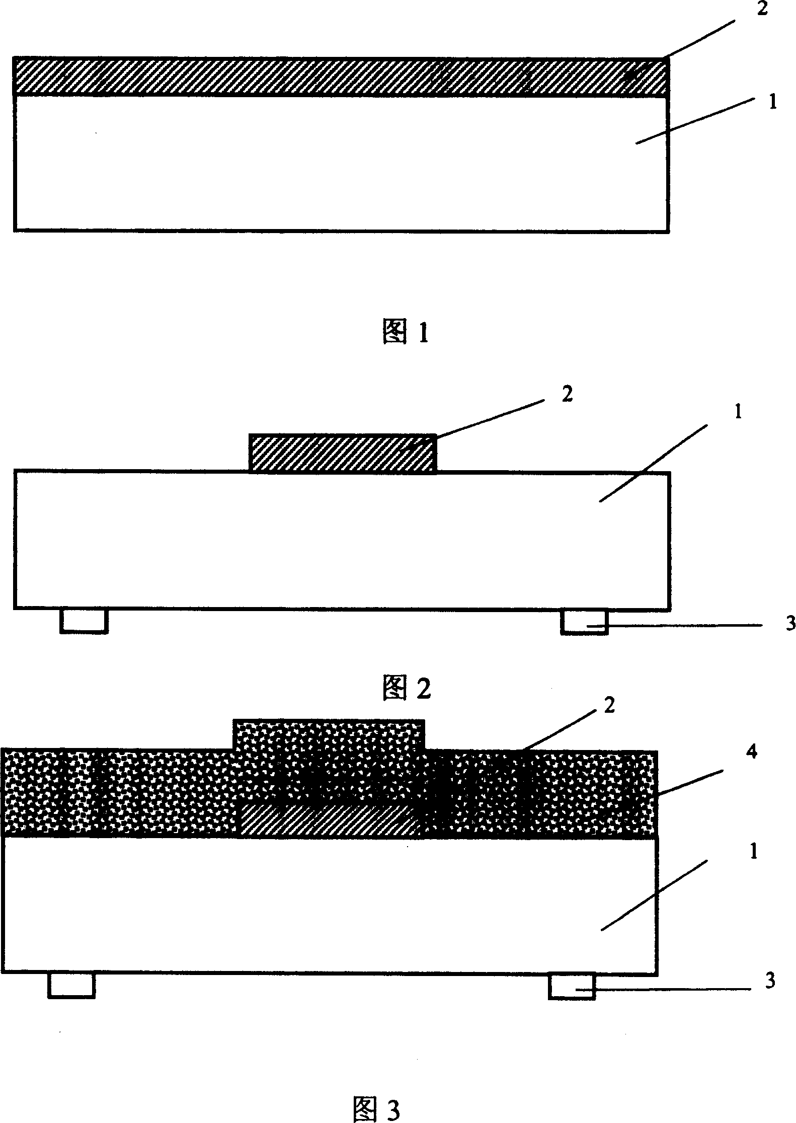
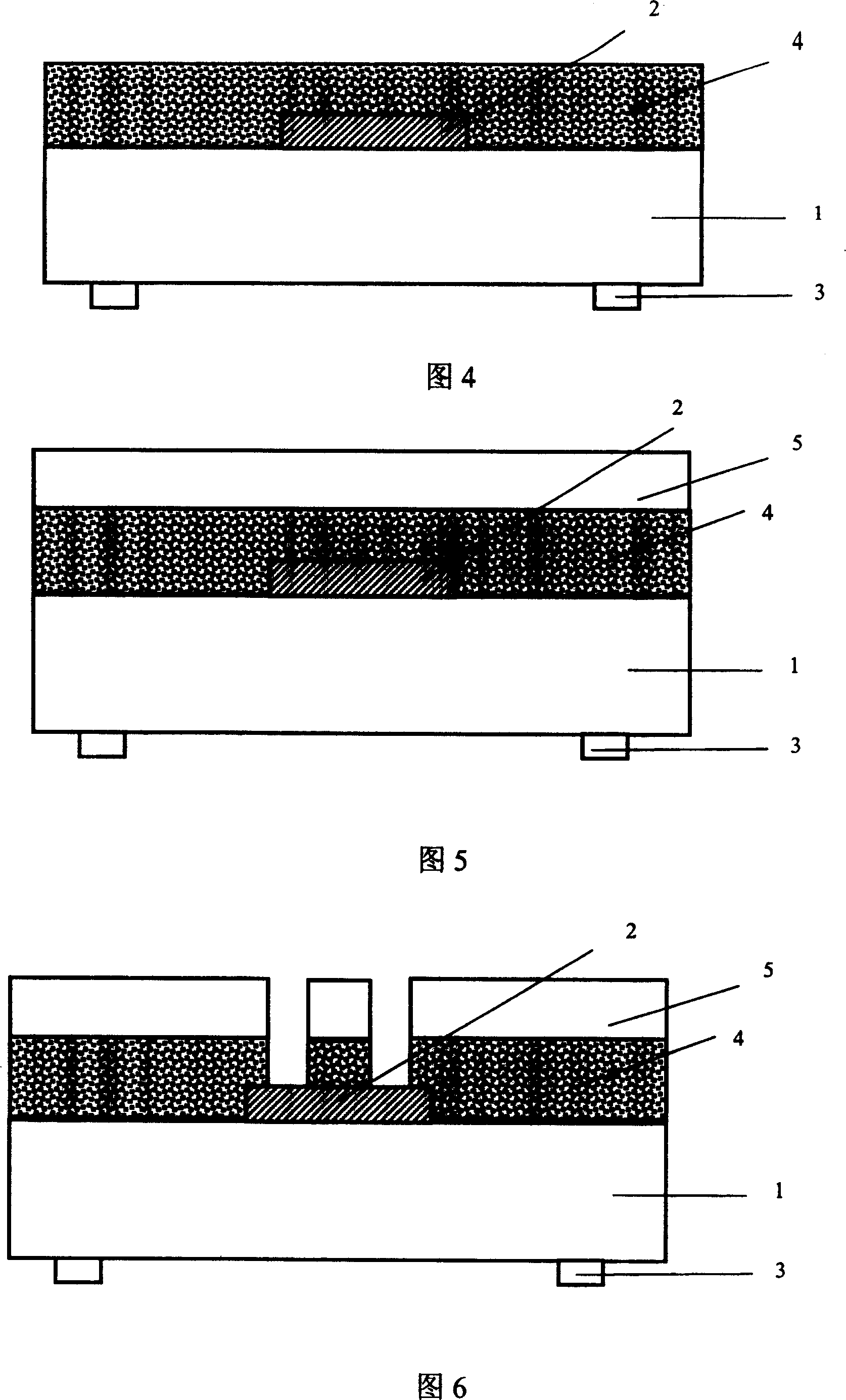
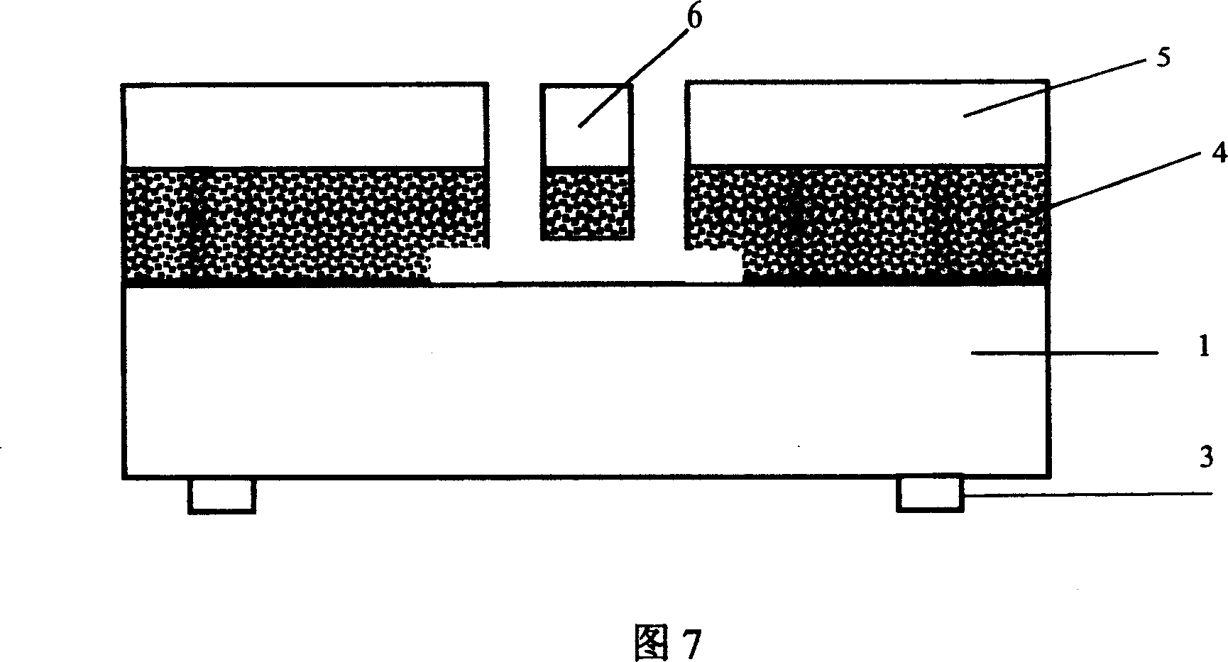
[0028] The manufacturing method steps of the MEMS sensor cantilever structure of the present invention are: preparing the first original silicon wafer 1 and the second original silicon wafer 5; adopting the repeated oxidation method on the first original silicon wafer 1 to form the oxide layer pattern 2 under the cantilever beam structure; Fabricate transition polysilicon layer 4; fabricate bonding sheet to form top layer silicon 5; release cantilever beam structure 6 by wet method.

[0029] 1. Prepare raw silicon wafers:

[0030] Using two double-sided polished first raw silicon wafers 1 and second raw silicon wafers 5, with a resistivity of 5-8Ω·cm, a crystal orientation, and a silicon wafer thickness of 400 μm;

[0031] 2. Form the oxide layer pattern 2 below the cantilever beam structure on the first original silicon wafer 1:

[0032] (1) At 900°C, 1 μm silicon dioxide...


PUM

PropertyMeasurementUnit
electrical resistivityaaaaaaaaaa
thicknessaaaaaaaaaa
thicknessaaaaaaaaaa

Abstract

The present invention relates to micro electronic mechanical system processing technology, and is especially making process of MEMS sensor cantilever structure. The making process includes the following steps: 1. preparing wafer; 2. forming the oxide layer pattern below cantilever structure via repeated oxidation on the first wafer; 3. making transition polysilicon layer; 4. making bonding chip to form top layer silicon structure; and 5. wet process of releasing cantilever structure. Compared with dry mass block releasing process, the present invention has no demerit of transverse etching of the mass block, has the advantages of obtaining relatively large mass block, no need of making netted cantilever structure for releasing, raised movable sensor cantilever sensitivity, reduced sensor volume, etc.

Description

(1) Technical field [0001] The invention relates to the field of micro-electro-mechanical system processing, in particular to a method for manufacturing a suspension beam structure of a MEMS sensor. (2) Background technology [0002] Micro-Electro-Mechanical Systems (MEMS) is the use of semiconductor technology to manufacture integrated mechanical and electronic components to achieve the purpose of miniaturization of the system. There are various processing techniques of MEMS, such as traditional body processing technique, surface sacrificial layer technique, combination of deep groove etching and bonding technique, SCREAM (Single Crystal Reactive Etching and Metallization) technique, LIGA technique, etc. Among them, the SCREAM process is used to manufacture micro-actuators or structures that move along the horizontal plane of the wafer. It can manufacture many silicon-based mesh or beam-type movable structures for mechanical sensing and other fields. However, the conventio...

Claims


Application Information

Patent Timeline
11 Jul 2007
Publication
CN1325367C
IPC
B81C1/00
Inventors
刘勇; 谭开洲