In-situ metal barrier deposition of sputter etching on interconnect structure

An etching and metal layer technology, applied in the direction of electrical components, semiconductor/solid-state device manufacturing, circuits, etc., can solve problems such as damage and wafer damage

Inactive Publication Date: 2007-08-15
INFINEON TECH AG +2
View PDF4 Cites 0 Cited by
  • Summary
  • Abstract
  • Description
  • Claims
  • Application Information

AI Technical Summary

Problems solved by technology

[0017] Wafers may also be damaged when conventional argon sputtering is performed on the metal layer. In the exemplary cross-sectional view of a wafer in FIG. , 300' includes a hard mask 301, an IDL 302, and a metal 303, after conventional argon sputtering cleaning, the wafer has been deposited on the field (field) 307', the trench bottom 302', and the gradual change Thin sidewall 306' metal may be removed and damage to hard mask 301' and IDL 302' and to etch profile 304' may occur, again, underlying metal may splatter onto the IDL 302 ' and deposited metal 305' over the

Method used


Image

  • In-situ metal barrier deposition of sputter etching on interconnect structure
  • In-situ metal barrier deposition of sputter etching on interconnect structure
  • In-situ metal barrier deposition of sputter etching on interconnect structure

Examples


Embodiment Construction

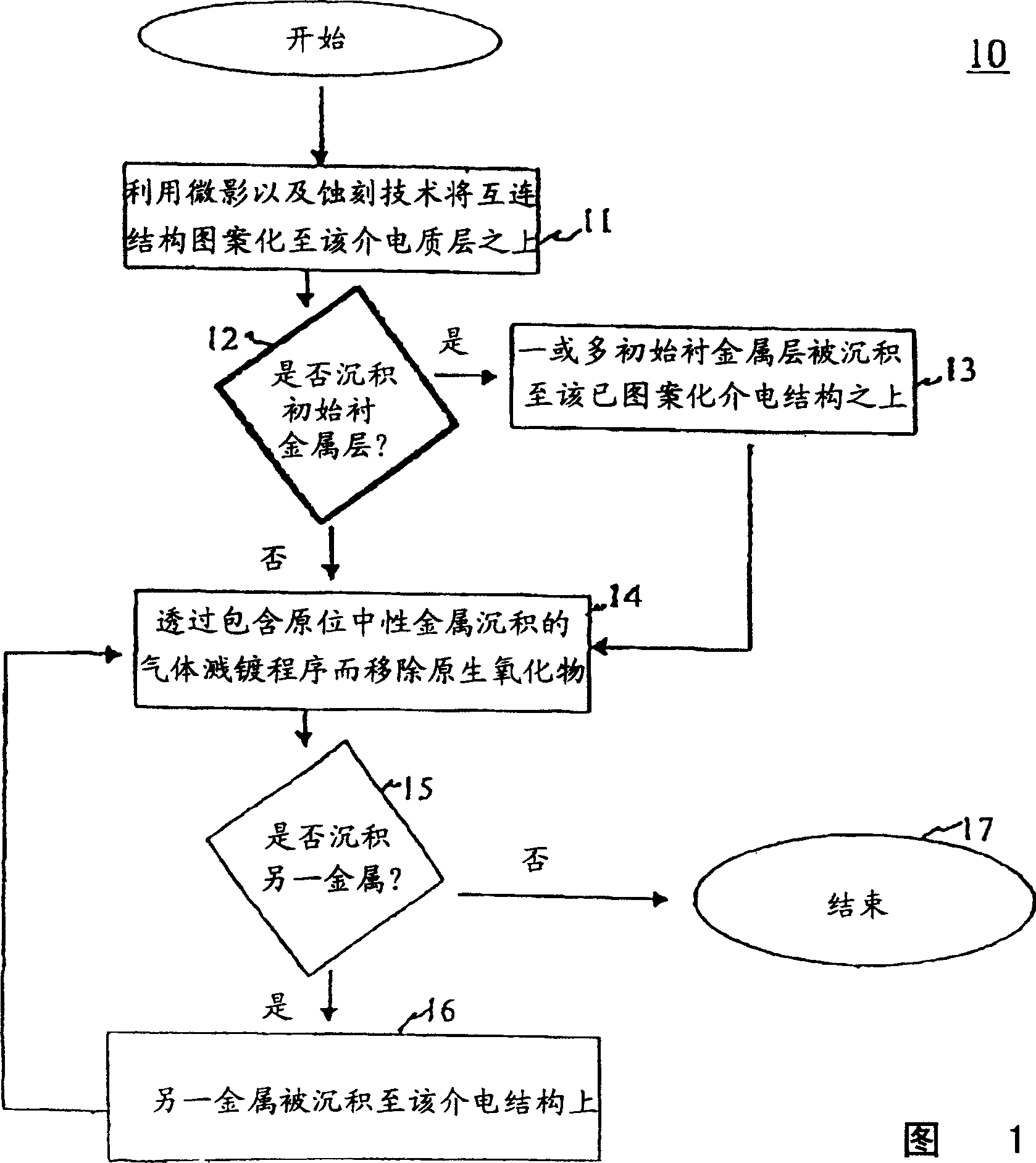
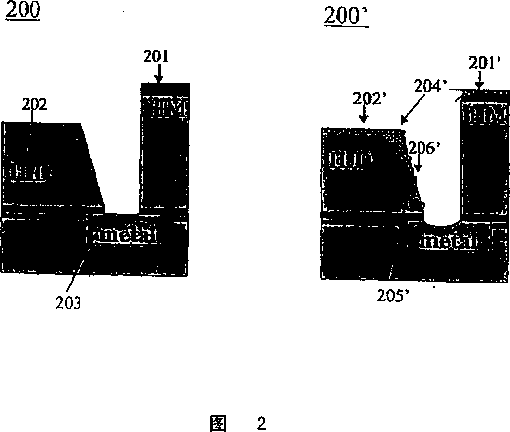
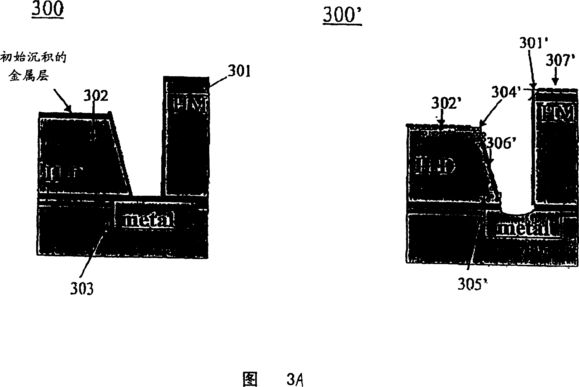
[0038] In accordance with embodiments of the present invention, gas sputtering cleaning procedures are provided to be performed on a patterned wafer that avoids or minimizes damage to the hard mask or to the IDL without compromising the etch profile Significant changes or spilled metal underneath onto the IDL.

[0039] In addition, an embodiment of the present invention provides a semiconductor device manufacturing method that advantageously utilizes a single deposition chamber.

[0040] As shown in flow diagram 10 in Fig. 1, the process begins with a semiconductor device (wafer) (not shown) having a dielectric layer on which micro An interconnect structure etched by lithography or etching techniques 11, such lithography and etching are well known in the art, the wafer is placed in a deposition chamber (not shown).

[0041] Then, it is determined whether the initial metal layer is to be deposited 12, if no initial metal layer is required, then the wafer can be placed in the d...


PUM

PropertyMeasurementUnit
thicknessaaaaaaaaaa

Abstract

A method of fabricating a semiconductor device having a dielectric structure on which an interconnect structure is optionally patterned using lithographic and etching techniques, within a single deposition chamber, is provided. The dielectric structure may optionally be covered by diffusion barrier materials prior to a sputter etching process. This sputter etching process is used to remove the native oxide on an underneath metal conductor surface and includes a directional gaseous bombardment with simultaneous deposition of metal neutral. Diffusion barrier materials may also be deposited into the pattern.

Description

technical field [0001] The present invention relates generally to semiconductor wafer fabrication. Background technique [0002] Increasing the density of semiconductor wafers has allowed more components to be placed on the wafer surface, which in turn has reduced the surface wiring area available for components, which has led to the use of multi-level metal layer stacks on the wafer Multilevel metallization schemes. A typical stack starts with a barrier layer formed by silicidation of the silicon surface to create a reduced resistance between the surface and the metal layers. [0003] And if aluminum is used as the conductive material of the metal layer, the barrier layers can avoid alloying between aluminum and silicon, both titanium-tungsten (TiW) and titanium nitride (TiN), and other materials are typically used as barrier layers. [0004] Occasionally, a platinum silicide layer is deposited on top of the exposed silicon prior to the deposition of titanium tungsten (T...

Claims


Application Information

Patent Timeline
Patent Type & Authority Patents(China)
IPC IPC(8): H01L21/285H01L21/443H01L21/768
CPCH01L21/76862H01L21/76865H01L21/76805H01L21/76838H01L21/76844
Inventor K·川恩达L·柯利文格尔A·考利方隼飞S·格利高A·H·西蒙T·斯布恩尔王允愈杨智超
Owner INFINEON TECH AG
Why Eureka
Try Eureka