Flash memory interface controller

A flash memory and interface controller technology, applied in the direction of instruments, electrical digital data processing, data processing input/output process, etc., can solve problems such as complex interface logic relationship, achieve flexible interface, wide application fields, and low cost Effect

Inactive Publication Date: 2002-09-04
长春迈思信息系统工程监理有限责任公司
View PDF0 Cites 4 Cited by
  • Summary
  • Abstract
  • Description
  • Claims
  • Application Information

AI Technical Summary

Problems solved by technology

The bus structure of NAND FLASH MEMORY adopts 8-bit address / data bus, which is different from the NOR structure of FLASH MEMORY, making the interface logic relationship complicated

Method used


Image

  • Flash memory interface controller
  • Flash memory interface controller
  • Flash memory interface controller

Examples


Embodiment Construction

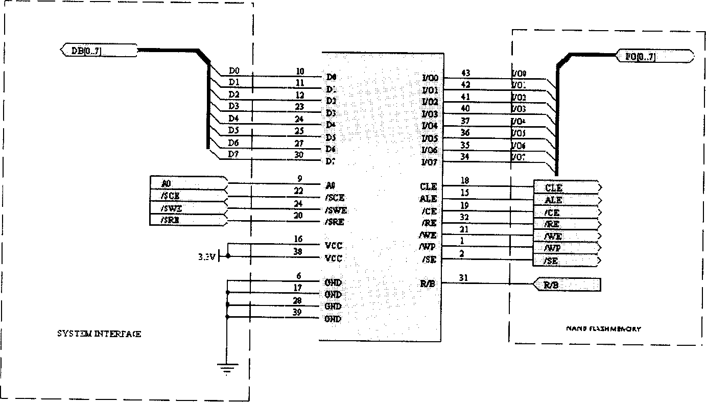
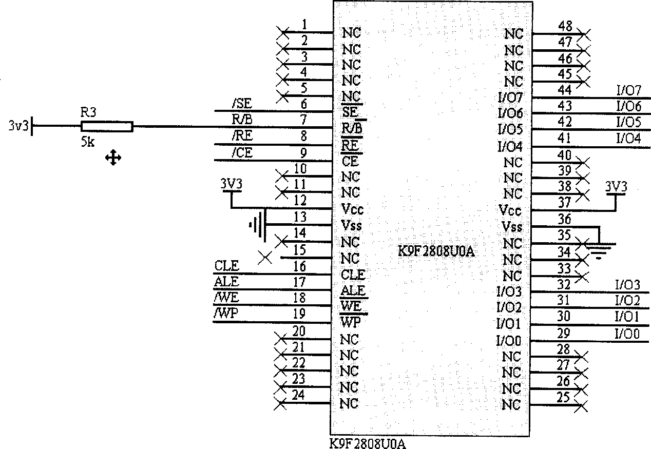
[0017] In this example, the flash memory (NAND FLASH MEMORY) uses SAMSUNG 8M * 8 BIT NAND FLASH MEMORY KM29U6400AT is an example, it is compatible with NAND FLASH MEMORY of other companies such as FUJI and TOSHIBA, and the NAND FLASH MEMORY of other companies is only different in chip capacity and package, and the signal interface logic is exactly the same.

[0018] The meaning of the interface signal of the flash memory (NAND FLASH MEMORY) interface controller is as follows: 1:

[0019] I / O[0..7]: NAND FLASH MEMORY interface controller and flash memory

[0020] The data input / output signal of the device (NAND FLASH MEMORY).

[0021] CLE: NAND FLASH MEMORY interface controller output to flash

[0022] The command latch signal of the memory (NAND FLASH MEMORY). When CLE is

[0023] When high, on the rising edge of / WE, the command is written to the flash memory through I / O[0..7]

[0024] (NAND FLASH MEMORY) command register.

[...


PUM


Abstract

The present invention relates to an interface control of nand flash memory in computer memory used for electronic instrument and equipment, and is characterized by that it utilizes the adoption of programmable logical device (CPLD) to make correspondent logic conversion, and according to the logical relationship between signals said programmable logical device utilizes the writing of logical equation to make logical simulation and logical emulation to form logical equation acceptable by programmable logical device, finally program it into the programmable logical device so as to make it obtain the function of logical conversion. At the same time, in order to meet the matching of voltage between signals said invention can provide conversion of power supply voltage. Said invention can make nand flash memory obtain more flexible application, including embedded system, for exampling PC and peripheral unit, telecommunication exchange and others.

Description

Technical field: [0001] The invention belongs to the technical field of computer storage, in particular to an interface controller used for flash memory (NAND FLASH MEMORY) in computer memory on electronic equipment. Background technique: [0002] Flash memory (Flash Memory) is a type of non-volatile memory NVM (Non-VolatileMemory) that can maintain on-chip information even after the power supply is turned off; and volatile memories such as DRAM and SRAM, when the power supply is turned off The information in the chip is lost immediately. Flash Memory integrates the characteristics of other types of non-volatile memory: Compared with EPROM, flash memory has obvious advantages - it is electrically erasable and reprogrammable in the system without requiring special high voltage (some first Generation flash memory also requires high voltage to complete erase and / or program operations); compared with EEPROM, flash memory has the characteristics of low cost and high density. It...

Claims


Application Information

Patent Timeline
Patent Type & Authority Applications(China)
IPC IPC(8): G06F3/00
Inventor 黄玉硕李英志
Owner 长春迈思信息系统工程监理有限责任公司
Why Eureka
Try Eureka