Polycrystalline silicon grading method and system and thin film transistor making method and system

A technology of thin film transistors and polysilicon, which is applied in the direction of transistors, semiconductor/solid-state device manufacturing, semiconductor devices, etc., can solve problems such as uneconomical time and cost, inability to determine the crystal state of polysilicon films, and difficulty in evaluating polysilicon films, etc., to achieve improvement The effect of manufacturing yield

Inactive Publication Date: 2002-09-25
JAPAN DISPLAY INC
View PDF0 Cites 5 Cited by
  • Summary
  • Abstract
  • Description
  • Claims
  • Application Information

AI Technical Summary

Problems solved by technology

[0006] However, as a method for evaluating polysilicon films, there is only known a more practical method of judging the crystal state of polysilicon films by picking up surface images using a spectroscopic ellipsometer, scanning electron microscope, etc., and visually inspecting the surface images thereof
This method cannot objectively determine the crystal state of the polysilicon film in a non-contact manner, and the time and cost are not cost-effective
Thus, this method is difficult to use for evaluating polysilicon films in process

Method used


Image

  • Polycrystalline silicon grading method and system and thin film transistor making method and system
  • Polycrystalline silicon grading method and system and thin film transistor making method and system
  • Polycrystalline silicon grading method and system and thin film transistor making method and system

Examples


Embodiment Construction

[0040] Hereinafter, preferred embodiments of a polysilicon film evaluation system and a polysilicon film evaluation method according to the present invention, and a thin film manufacturing system using the polysilicon film evaluation system and a thin film manufacturing method using the polysilicon film evaluation method will be described with reference to the accompanying drawings.

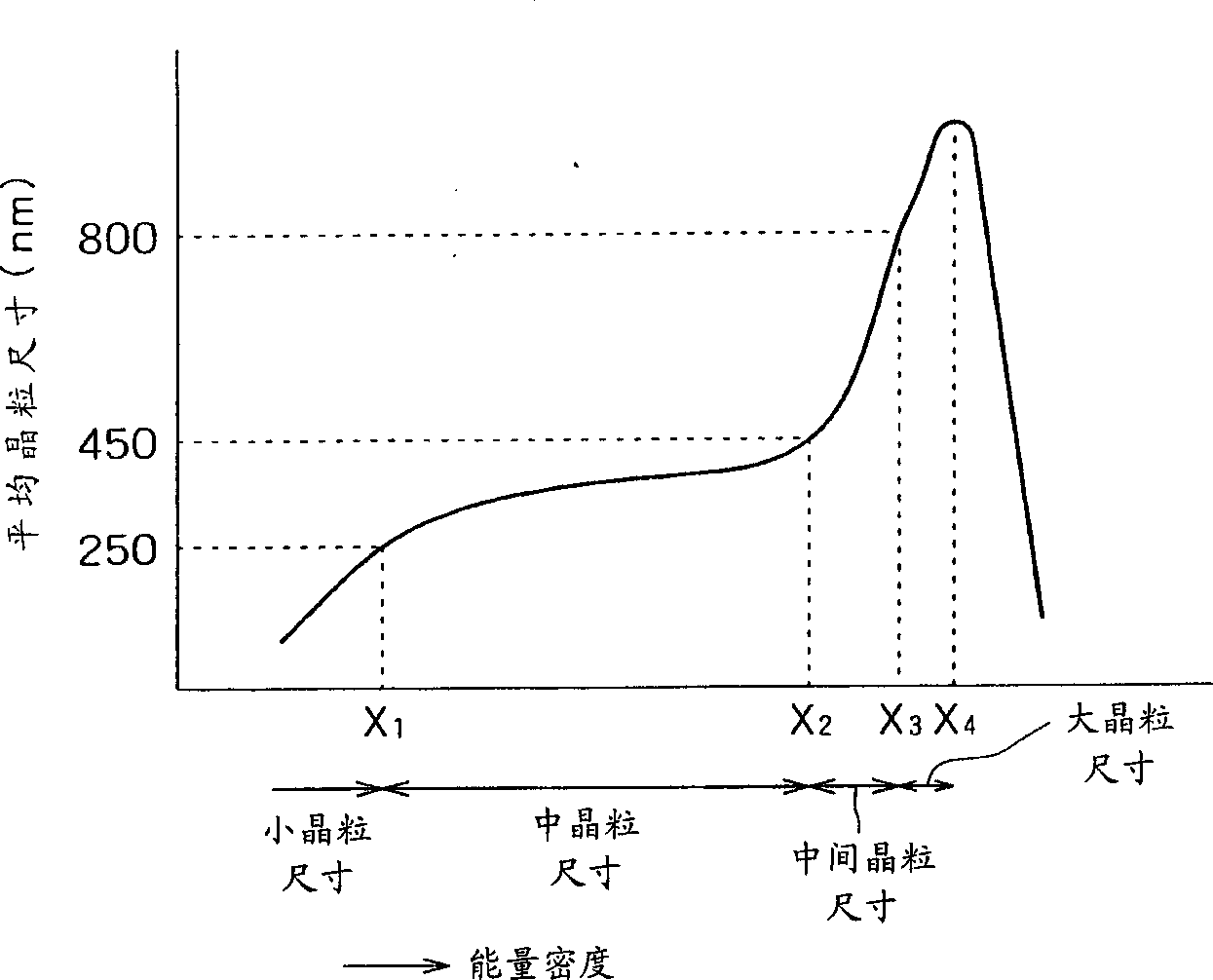
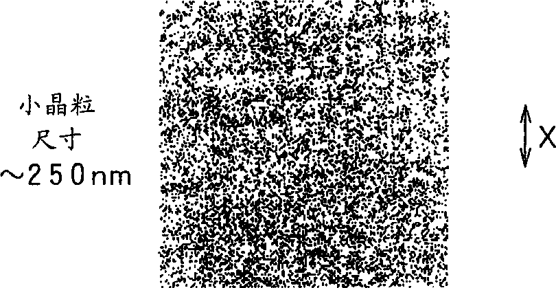
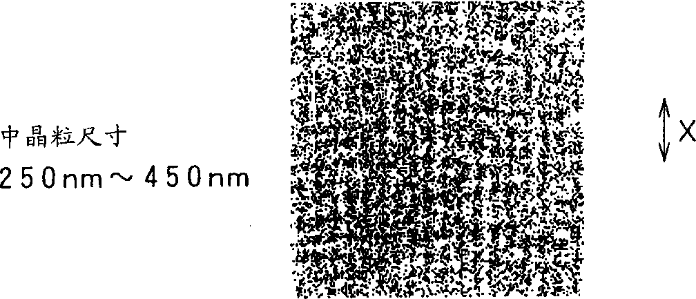
[0041] A polysilicon film evaluation system according to an embodiment of the present invention is generally used to inspect a polysilicon film formed in the process of manufacturing a thin film transistor having a top gate structure (hereinafter referred to as "top gate type TFT"). For example, a top-gate type TFT is constituted by stacking a polysilicon film (channel layer), a gate insulating film, and a gate electrode in this order from the substrate side on a glass substrate. In other words, in a top gate type TFT, a polysilicon film functioning as a channel layer is formed at the lowest layer...


PUM

PropertyMeasurementUnit
particle sizeaaaaaaaaaa

Abstract

A method for evaluating the state of a polysilicon film objectively, accurately, and automatically in a non-contact manner is provided. The method includes the steps of: picking up the surface of the polysilicon film formed by excimer laser annealing; dividing the picked-up image into grids (mesh) each having a specific size; calculating the contrast of each grid; extracting the picked-up The highest contrast value and the lowest contrast value in the image, the contrast ratio between them is calculated and the average grain size of the polysilicon film is judged on the basis of the contrast ratio.

Description

technical field [0001] The present invention relates to a polysilicon evaluation method for evaluating the crystal state of a polysilicon film and a polysilicon film evaluation system therefor, and to a thin film transistor having a polysilicon film formed by annealing amorphous silicon and a thin film transistor manufacturing system therefor. Background technique [0002] In recent years, thin film transistors using a polysilicon film as a channel layer have come into practical use. A thin film transistor using a polysilicon film as a channel layer exhibits high field mobility, so that, if used as a driving circuit for a liquid crystal display or the like, such a thin film transistor can realize higher definition, higher operating speed and display miniaturization. [0003] On the other hand, in recent years, so-called low-temperature polycrystallization treatment has been developed. In this process, a polysilicon film is formed by heat-treating a...

Claims


Application Information

Patent Timeline
Patent Type & Authority Applications(China)
IPC IPC(8): G01N15/02G01N21/84G01N21/95H01L21/20H01L21/268H01L21/336H01L21/66H01L29/786
CPCG01N21/95H01L29/66757H01L29/78675H01L22/00
Inventor 和田裕之梅津畅彦田附幸一
Owner JAPAN DISPLAY INC
Why Eureka
Try Eureka