Novel button anti-reflection film structure
A bottom anti-reflection, thin-film structure technology, which is applied in the photoengraving process, optics, instruments, etc. of the patterned surface, can solve the problem of poor process stability of process development, changes in the thickness of photoresist on the surface of silicon wafers, and depth of field during photolithography. impact, etc.
Inactive Publication Date: 2002-12-18
SHANGHAI HUA HONG GROUP
View PDF0 Cites 7 Cited by
- Summary
- Abstract
- Description
- Claims
- Application Information
AI Technical Summary
Problems solved by technology
Of course, due to the use of PECVD method, it is worse than organic BARC in terms of process development and process stability.
In addition, the use of inorganic BARC will cause changes in the thickness of the photoresist on the surface of the silicon wafer, which will also have a certain impact on the uniformity of the line width and the depth of field during photolithography.
Method used
View moreImage
Smart ImageViewing Examples
Examples
Embodiment Construction
[0014] The implementation process of the present invention is:
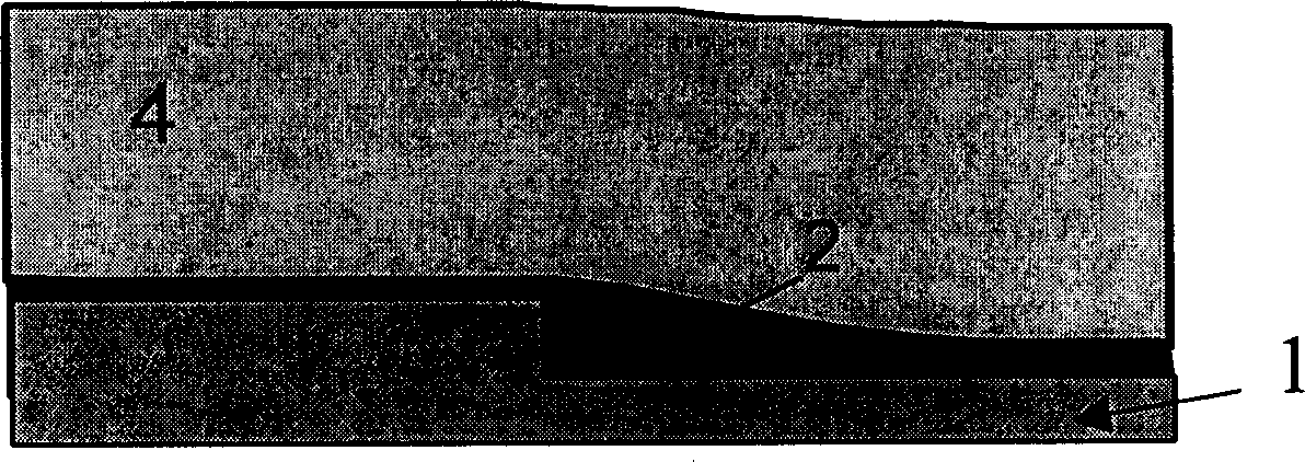
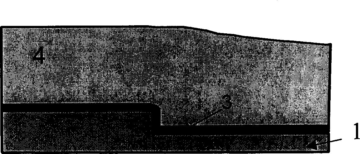
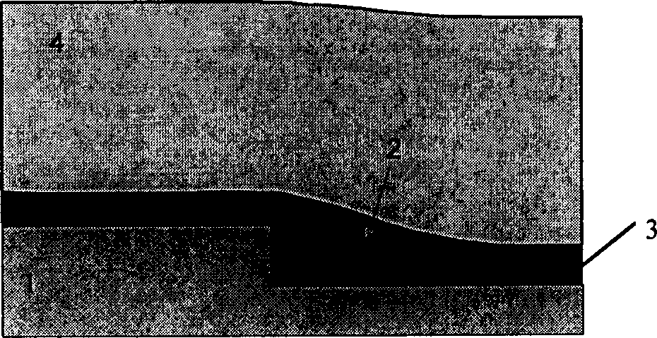
[0015] 1. Use PECVD to deposit inorganic BARC (such as SiON) on the surface of the silicon wafer with a thickness of about 35nm;
[0016] 2. Use the spin-on method to coat organic BARC on the surface of the silicon wafer, such as the products of Clariant or Shipley; the thickness is about 100nm. That is, a composite reflective film structure with good performance is obtained.
[0017] 3. Then apply photoresist on the surface of organic BARC; and complete photolithography and complete etching.
[0018] The composite anti-reflection film improves the quality of photolithography, reduces the line width loss of traditional etching, and improves the process stability.
Login to View More PUM
| Property | Measurement | Unit |
|---|---|---|
| thickness | aaaaa | aaaaa |
| thickness | aaaaa | aaaaa |
| thickness | aaaaa | aaaaa |
Abstract
This invention applies a technique of a base anti-reflection film (BARC) composed of organic BARC and inorganic BARC. This invention puts forward a complex anti-reflection structure combined organic and inorganic BARC with the inorganic BARC under the organic BARC which utilizes either the advantage of organic BARC flat or reduces wide line loss in the traditional organic BARC etching since inorganic BARC etching since inorganic BARC of good selection is used.
Description
technical field [0001] The invention belongs to the technical field of integrated circuit manufacturing technology, and in particular relates to a bottom anti-reflection film structure. Background technique [0002] With the continuous development of integrated circuits, the minimum line width of transistors continues to shrink. The current mainstream technology of 0.18 μm means that the length of the gate is 0.18 μm. The continuous reduction of line width firstly requires that the lines defined by the photolithography process become narrower and narrower, and of course the requirements for the etching process are also higher and higher. In order to meet the requirements of lithography, in addition to the continuous upgrading of lithography equipment, people also use other technologies to improve the quality and precision of lithography, and the use of anti-reflection coating (ARC) is one of them. The role of ARC is to prevent light from being reflected at the substrate int...
Claims
Login to View More Application Information
Patent Timeline
 Patent Type & Authority Applications(China)
IPC IPC(8): G03F7/00H01L21/027H01L21/31H01L21/469
Inventor 胡恒升
Owner SHANGHAI HUA HONG GROUP


