

High-voltage-resistant semiconductor device
A semiconductor, high withstand voltage technology, applied in the direction of semiconductor devices, transistors, electric solid devices, etc., can solve the problem of withstand voltage drop of high withstand voltage semiconductor devices
- Summary
- Abstract
- Description
- Claims
- Application Information
AI Technical Summary
Problems solved by technology
Method used
Image

Examples
Embodiment 1
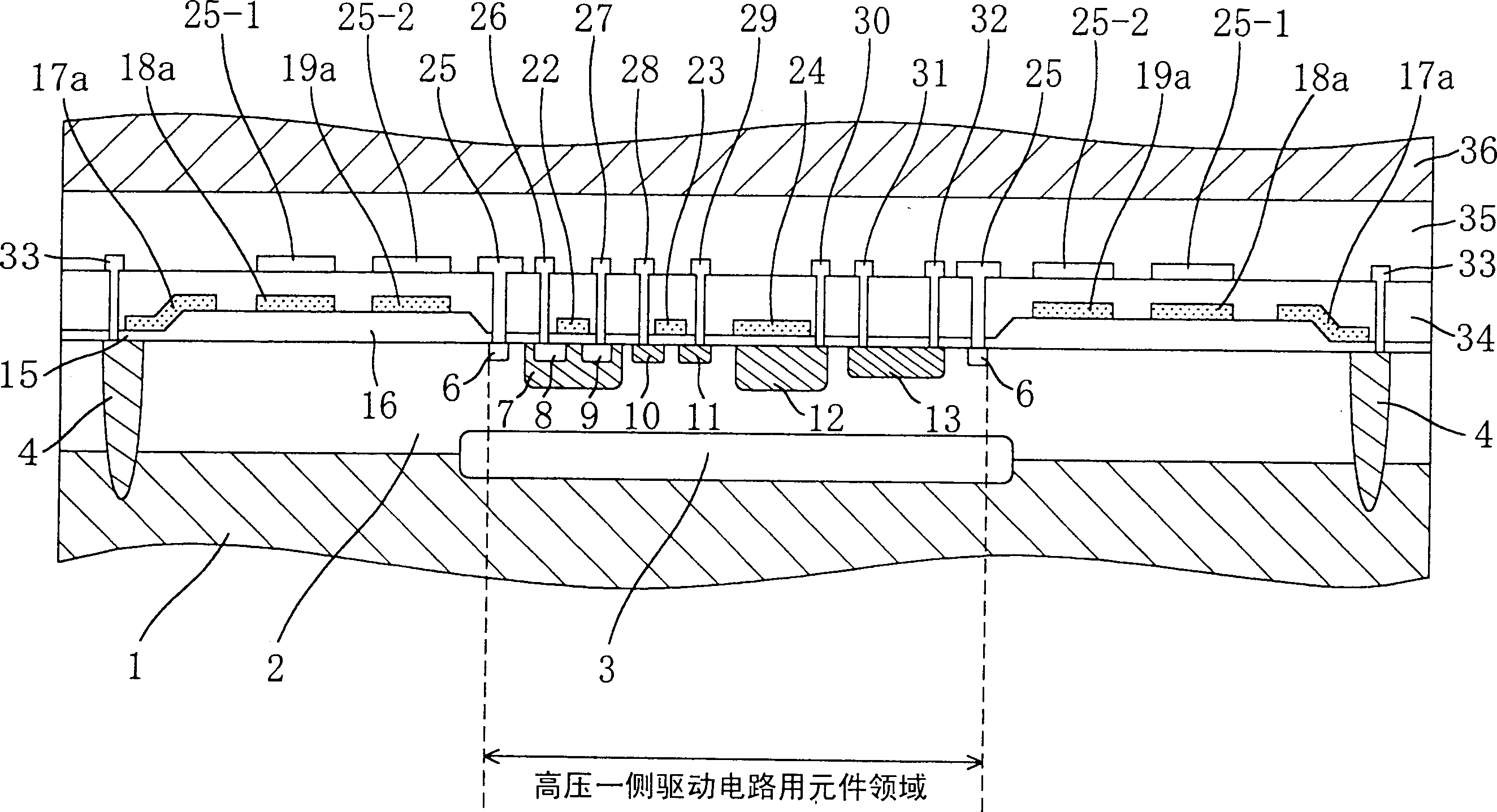
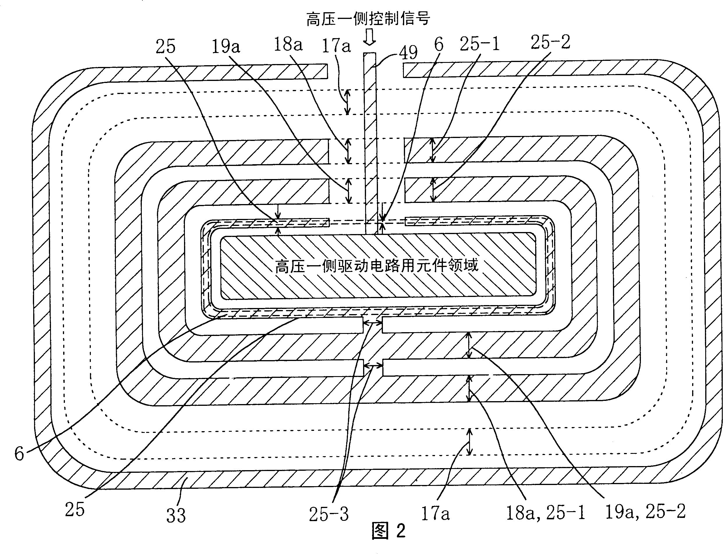
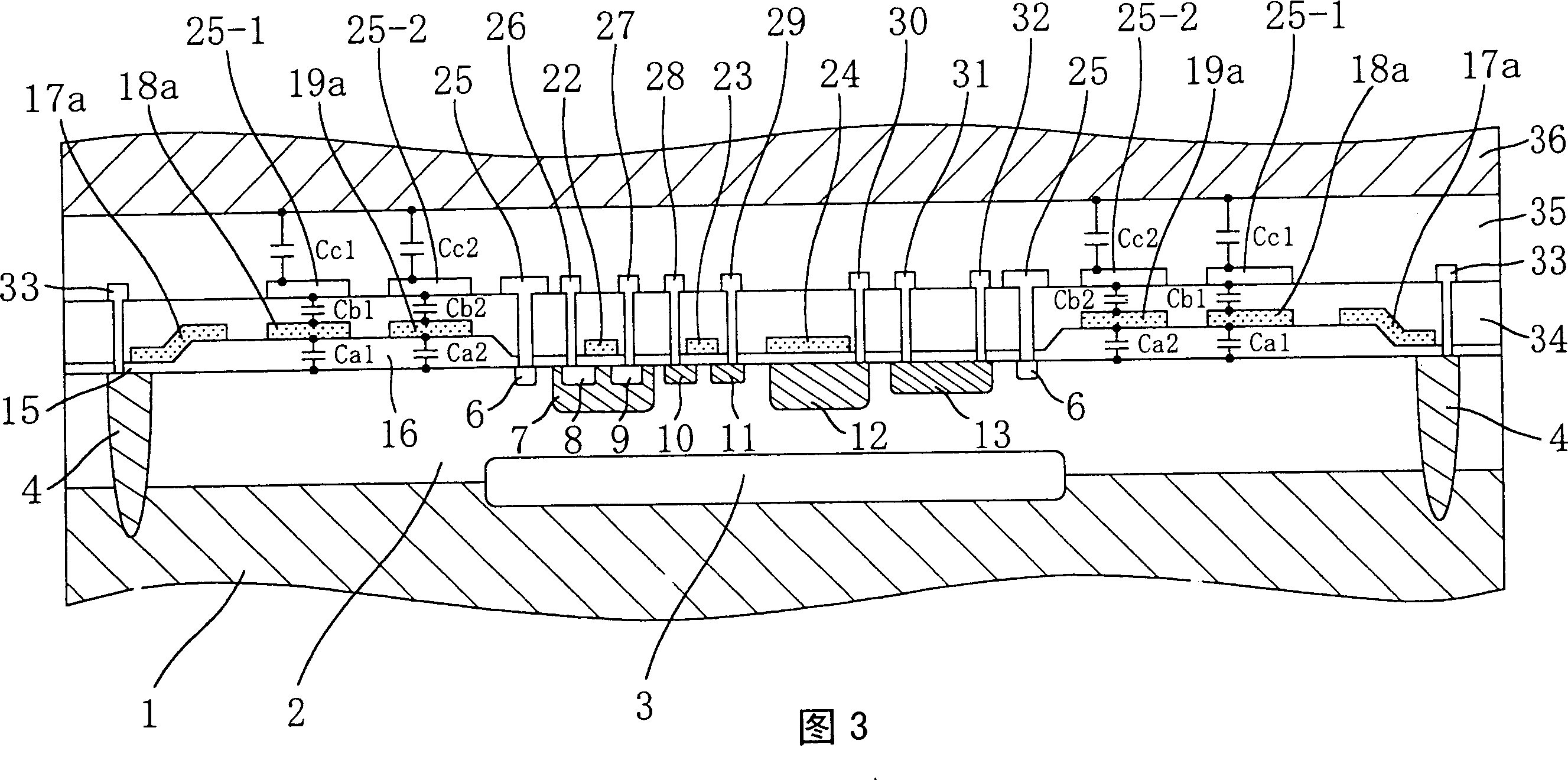
[0080] Below, refer to figure 1 Turning to FIG. 3, the high withstand voltage semiconductor device in Embodiment 1 will be described. figure 1 Fig. 2 schematically shows the cross-sectional structure of the high withstand voltage semiconductor device of the present embodiment, and FIG. 2 schematically shows the planar structure of the high withstand voltage semiconductor device of the present embodiment. In FIG. 2, only the silicone-made plate electrodes, metal electrodes, and N-type diffusion regions for contact are shown for easy viewing.
[0081] figure 1In the shown high withstand voltage semiconductor device, the plate electrodes 18a, 19a and a part (25-1, 25-2) of the metal electrodes provided through the interlayer insulating film 34 on them are capacitively coupled to each other, so as to prevent the The withstand voltage drops. The principle of preventing the withstand voltage drop at high temperature will be described later. The high withstand voltage semicond...
Embodiment 2
[0104] FIG. 5 schematically shows the cross-sectional structure of the high withstand voltage semiconductor device in the second embodiment. In this embodiment, different from the above embodiments, the lateral width of the metal electrodes 25-1, 25-2 is 1 / 2 of the plate electrodes 18a, 19a.
[0105] If the same verification as in Example 1 is carried out to the high withstand voltage semiconductor device of Example 2, in the structure of this example, because the potential (about 240V) of the semiconductor region 2 directly below the plate electrode 18a is in contact with the metal electrode 25 The potential difference of -1 voltage 600V is divided by the series circuit of Ca1 and Cb1 to obtain the potential difference (about 120V) between the plate electrode 18a and the semiconductor field 2, so the plate electrode 18a is about 360V. In addition, if the potential of the plate electrode 19a is verified, the potential is about 530V. This is because the potential is obtained b...
Embodiment 3
[0113] FIG. 6 schematically shows the cross-sectional structure of the main part of the high withstand voltage semiconductor device in the third embodiment. In the present example, unlike the second example, the ratio of capacitive coupling between plate electrodes and metal electrodes and capacitive coupling between plate electrodes and the semiconductor field 2 is different for each plate electrode. According to this structure, even if the insulating property of the surface protection film 35 is impaired, the influence on the plate electrode 19a on the high potential side can be reduced.
[0114] In the structure shown in FIG. 6, the lateral width of the ring-shaped metal electrode 25-1 is 1 / 2 of that of the plate electrode 18a, and the lateral width of the ring-shaped metal electrode 25-2 is increased. In short, the lateral width of ring-shaped metal electrode 25 - 2 is widened so as to cover the entire upper surface of plate electrode 19 a closest to N-type diffusion regio...
PUM
 Abstract
Description
Claims
Application Information