Multiphase clock transfer circuit and method

A technology of multi-phase clock and clock generation circuit, which is applied in the direction of electric pulse generator circuit, transmission system, electrical components, etc., and can solve the problems of increased clock time lag, increased wiring area, and wrong operation of circuits, etc.

Inactive Publication Date: 2003-09-03
SOCIONEXT INC
View PDF1 Cites 10 Cited by
  • Summary
  • Abstract
  • Description
  • Claims
  • Application Information

AI Technical Summary

Problems solved by technology

[0003] However, if the multi-phase clock is transmitted by the conventional method, in order to transmit the clock of each phase separately, when transmitting the clock of M phases (m is a natural number), m wires are required. As m becomes larger, the wiring area increases accordingly.
[0004] In addition, if the distance to transmit the clock is long, in general, the difference in the route length between the clocks of each phase will increase, and the influence of interference with other signal lines will also increase. The skew between the clocks will increase
[0005] Also, if the frequency of the clock is high, the ratio of the asymmetry between the clocks of the transmitted phases to the clock period will increase
For this reason, the phase relationship between the clocks of each phase cannot be guaranteed in each circuit unit block receiving multi-phase clocks, resulting in erroneous operation of the circuit

Method used


Image

  • Multiphase clock transfer circuit and method
  • Multiphase clock transfer circuit and method
  • Multiphase clock transfer circuit and method

Examples


Embodiment 1

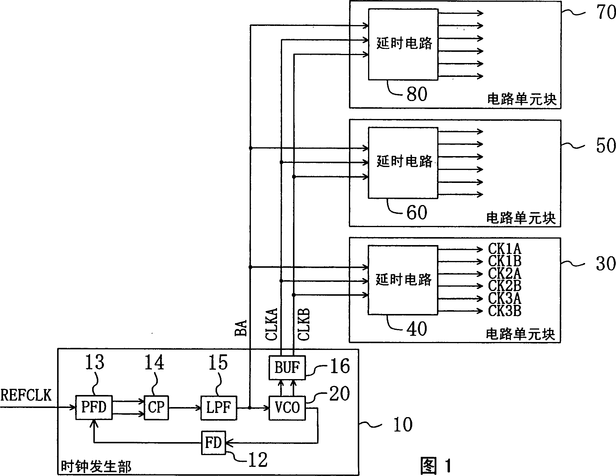
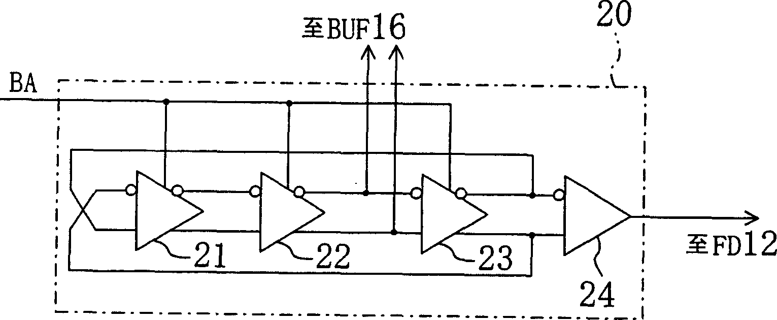
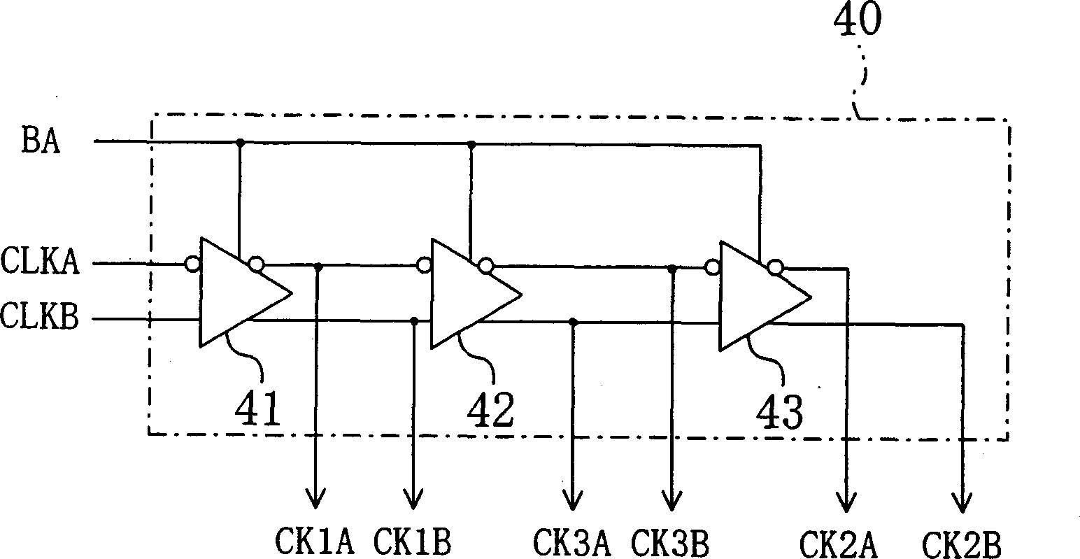
[0059] 1 is a block diagram of a semiconductor integrated circuit having a multiphase clock transfer circuit according to Embodiment 1 of the present invention. In FIG. 1 , the multiphase clock transfer circuit has a clock generation section 10 and delay circuits 40 , 60 and 80 . The delay circuits 40, 60 and 80 include clock circuit unit blocks 30, 50 and 70, respectively. The circuit unit blocks 30, 50, and 70 all employ multi-phase clocks for signal processing and the like.

[0060] The clock generating unit 10 has a frequency divider (FD) (frequency divider) 12, a phase frequency comparator (PFD) (phase frequency detector) 13, a charge pump (CP) 14, a low-pass filter (LPF) 15, a buffer ( BUF) 16 and a voltage controlled oscillator (VCO) (voltage controlled oscillator) 20 as a clock generating circuit. The phase-frequency comparator 13 and the charge pump 14 operate as a phase comparison circuit. The phase-frequency comparator 13, the charge pump 14, the low-pass filter ...

Embodiment 2

[0110] When the distance between the clock generation unit and the circuit block is large, variations in transistor characteristics are likely to occur, and inconsistencies in power supply potentials and ground potentials are also likely to occur. In this case, the delay amount of the clock generation part and the delay unit of a segment on the circuit unit block will not be consistent. In order to avoid the occurrence of this kind of situation, a circuit for correcting delay is installed on the delay circuit.

[0111] Figure 12 It is a circuit diagram of the delay circuit of the multi-phase clock transmission circuit according to Embodiment 2 of the present invention. Figure 12 The delay circuit has an alternative to the image 3 The delay units 341, 342 and 343 of the delay units 41-43 on the delay circuit 40 also have a delay correction circuit 345. The delay correction circuit 345 has a phase comparator (PD) 346 , a charge pump (CP) 347 and a low-pass filter (LPF) 348...

Embodiment 3

[0126] In the above embodiments, the technique for maintaining the frequency of the clock and the phase difference between multi-phase clocks in each circuit block has been described. In Embodiment 3, a technique for matching the phases of clocks between different circuit block blocks will be described. For example Figure 8 As shown, when the clock CKDA / CKDB is transmitted to each circuit unit block using a buffer, the phase inconsistency of the clock input to each circuit unit block will arise. This is because not only the distance from the clock generation unit to each circuit block is different, but also the number of buffers through which the clock passes differs depending on the circuit block.

[0127] Figure 14 It is a block diagram of an integrated circuit with a multi-phase clock transmission circuit according to Embodiment 3 of the present invention. exist Figure 14 , the multiphase clock transfer circuit has Figure 8 Clock generator 110, buffers 501, 502, 503,...


PUM


Abstract

A multi-phase clock transmission circuit includes: a clock generator for generating a clock synchronizing with a reference clock and a control signal responsive to the phase difference between the reference clock and the generated clock; and a delay circuit for generating a multi-phase clock based on the clock and the control signal. The clock generator generates a signal having a frequency equal to an integral multiple of the frequency of the reference clock and outputs the signal as the clock. The delay circuit has a circuit receiving the clock and including a plurality of delay elements in cascade connection each giving a delay according to the control signal to an input signal. Signals output from the plurality of delay elements are used as signals constituting the multi-phase clock.

Description

technical field [0001] The present invention relates to clock transfer technology in semiconductor integrated circuits. Background technique: [0002] In a semiconductor integrated circuit, a plurality of clocks having the same frequency and maintaining a predetermined phase difference can be used. Such multiple clocks are called polyphase clocks. When a multiphase clock is used, conventionally, a clock generation circuit configured with a PLL (phase locked loop: phase locked loop) or the like generates and outputs a multiphase clock. Then, the multi-phase clocks are distributed to the required circuit unit blocks through the dedicated wiring for transmitting the respective phase clocks. An example of such a technique is disclosed in JP-A-2-255908. [0003] However, if the multi-phase clock is transmitted by the conventional method, in order to transmit the clock of each phase separately, when transmitting the clock of M phases (m is a natural number), m wires are require...

Claims


Application Information

Patent Timeline
Patent Type & Authority Applications(China)
IPC IPC(8): H03K5/13H03K5/15H03L7/07H03L7/08H03L7/081
CPCH03L7/07H03L7/0814H03K5/133H03L7/0805H03K5/1504H03L7/0812H03L7/08H03L7/0816
Inventor 平田贵士岩田徹
Owner SOCIONEXT INC
Why Eureka
Try Eureka