

Process for preventing heavy duty optical resistance from collapsing
A technology for heavy industry light and photoresist, applied in photosensitive material processing, electrical components, semiconductor/solid-state device manufacturing, etc., can solve the problems of reduced production capacity, complex process, and increased production time
- Summary
- Abstract
- Description
- Claims
- Application Information
AI Technical Summary
Problems solved by technology
Method used
Image

Examples
Embodiment Construction
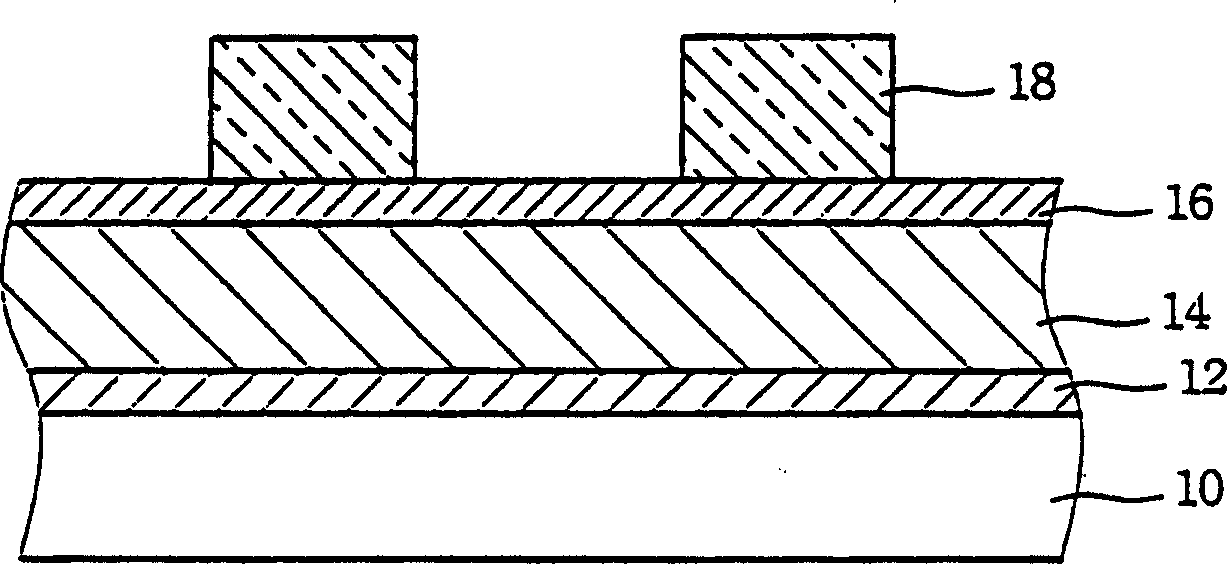
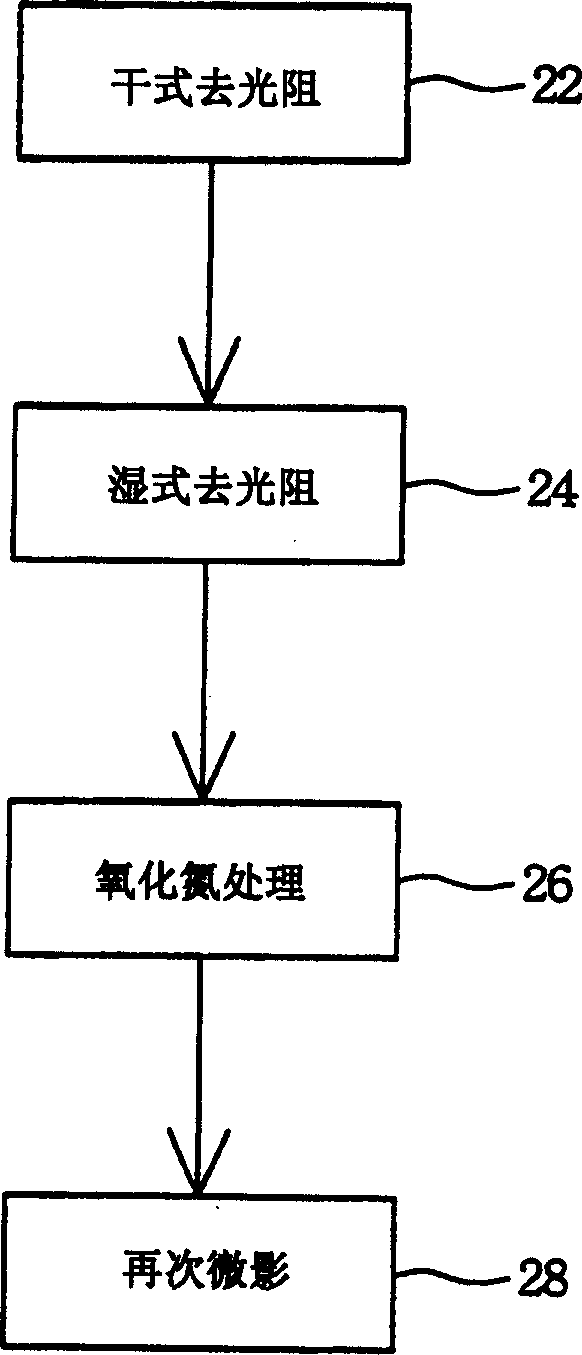
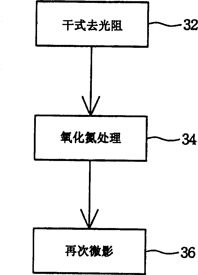
[0021] The present invention discloses a method for preventing the collapse of photoresist in heavy industry, and the method of the present invention will be described below in the form of a preferred embodiment.
[0022] Please refer to figure 1 , which shows a cross-sectional schematic diagram of a process for forming a gate of a transistor. A gate oxide layer 12 is formed on a semiconductor substrate 10 . Preferably, the gate oxide layer 12 can form a layer of silicon dioxide (SiO 2 ). Next, a polysilicon layer 14 is formed on the gate oxide layer 12 . The polysilicon layer 14 can be formed by chemical vapor deposition with a thickness of about 500-5000 angstroms, preferably 2000 angstroms. Subsequently, an anti-reflective coating (Anti-Reflective Coating, ARC) 16 is covered on the polysilicon layer 14 . Preferably, the anti-reflection coating layer 16 can be deposited on the polysilicon layer 14 by a chemical vapor deposition method of silicon oxynitride (SiON) materi...
PUM
| Property | Measurement | Unit |
|---|---|---|
| thickness | aaaaa | aaaaa |
| reflectance | aaaaa | aaaaa |
Abstract
Description
Claims
Application Information