

Single-electron storage designed based on coulomb damping principle and its preparing method
A principle design, Coulomb blocking technology, applied in the direction of electric solid-state devices, semiconductor/solid-state device manufacturing, circuits, etc., can solve the problems of low operating temperature of storage devices, high power consumption of devices, and restrictions on the further improvement of integration
- Summary
- Abstract
- Description
- Claims
- Application Information
AI Technical Summary
Problems solved by technology
Method used
Image

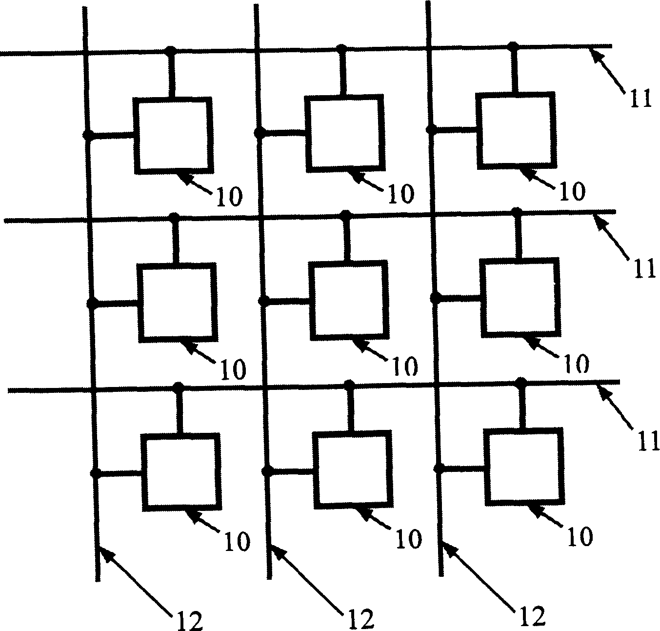
Examples
Embodiment 2
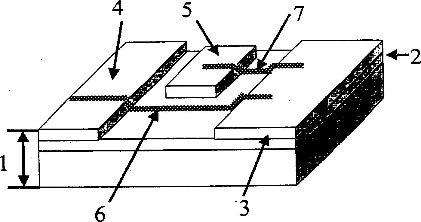
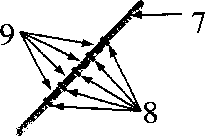
[0030] The preparation method of the source electrode 3, the drain electrode 4 and the gate electrode 5 is the same as that of embodiment 1, except that the thickness of the silicon layer on the surface of the SOI after thinning is 5 or 500 nanometers; the source The distance between the pole electrode and the drain electrode is 5 nanometers or 1 micrometer; the gate area is between 1 square nanometer and 1 square micrometer. And on the inner side of the drain electrode 4 and the outer side of the gate electrode 5, a catalyst region 13 is placed, and the catalyst region 13 is made of Fe, Co, Ni or an alloy thereof, such as Figure 9 As shown, carbon nanotubes are grown in situ toward the direction of the source electrode 3 , and the other end of the grown carbon nanotubes is in contact with the source electrode 3 . In addition, the probe technology of the atomic force microscope is used to deform the carbon nanotube 7 locally to form a tunnel junction 8 with a distance of 10 n...
PUM
| Property | Measurement | Unit |
|---|---|---|
| Thickness | aaaaa | aaaaa |
Abstract
Description
Claims
Application Information