Plasma etching method and device

A plasma and etching device technology, applied in semiconductor/solid-state device manufacturing, electrical components, circuits, etc., can solve the problems of increasing electrode size, complexity or power consumption, and improve uniformity , the effect of increasing plasma density

Inactive Publication Date: 2004-02-25
TOKYO ELECTRON LTD
View PDF2 Cites 15 Cited by
  • Summary
  • Abstract
  • Description
  • Claims
  • Application Information

AI Technical Summary

Problems solved by technology

However, recently, the size of the substrate to be processed has been increased, and the size of the electrode has been increased significantly. The disadvantages derived from this (enlargement and complexity of the cooling mechanism, or increase in power consumption, etc.) are too large, and it cannot be said to be effective or practical. the solution

Method used


Image

  • Plasma etching method and device
  • Plasma etching method and device
  • Plasma etching method and device

Examples


Embodiment Construction

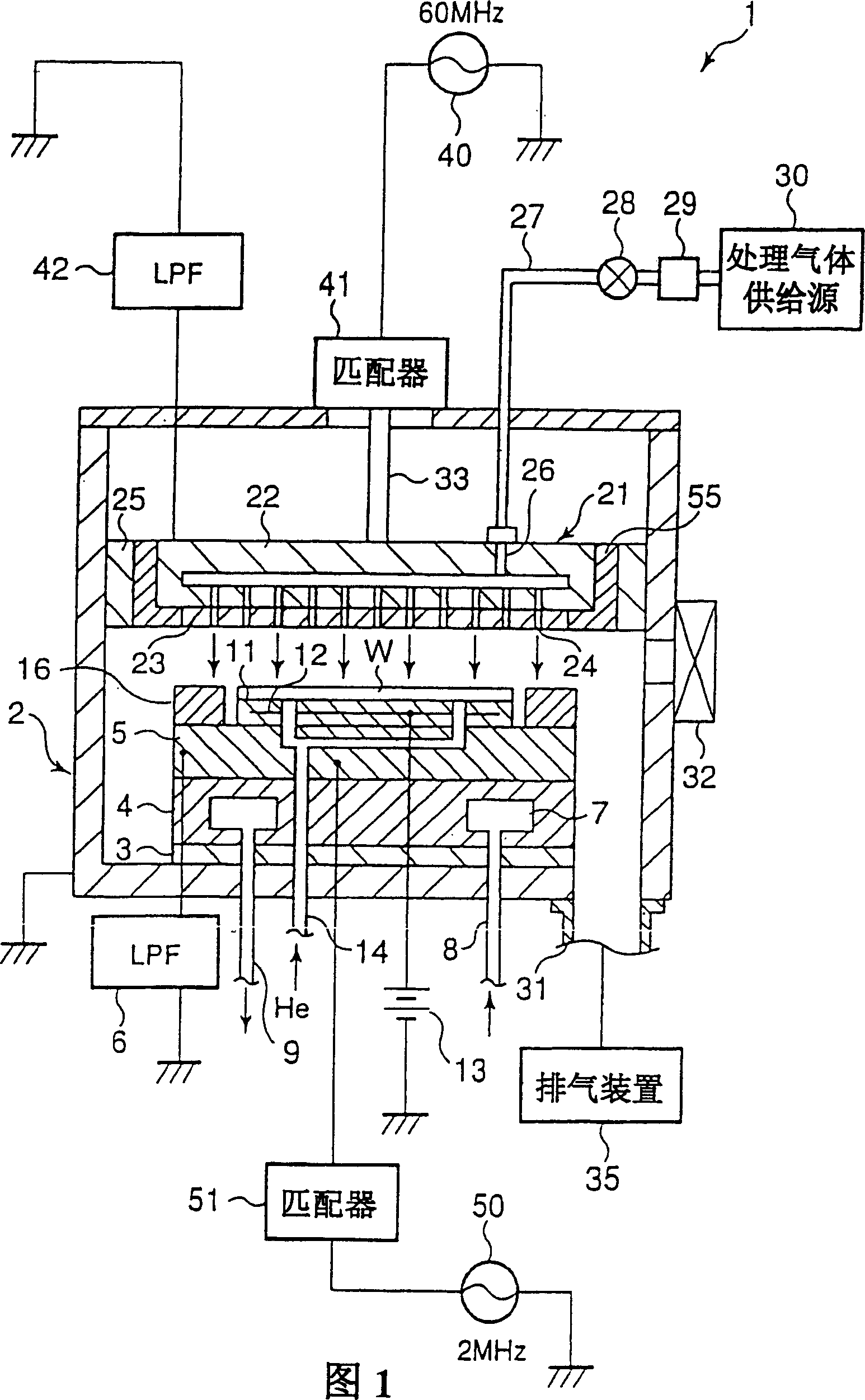
[0039] Refer to Figure 1- Figure 14 Embodiments of the plasma etching method and apparatus of the present invention will be described.

[0040] Figure 1 to image 3 An embodiment of the plasma etching method is shown, and FIG. 1 shows a plasma device used in the plasma etching method. On the bottom of this plasma 1 grounded treatment chamber 2 , an insulating support plate 3 is laid, on which support plate 3 an inductor 5 is arranged by means of a support table 4 . The inductor 5 constitutes a lower electrode on which a substrate to be processed (object to be etched), for example, an electrostatic chuck 11 for chucking and holding a wafer W while holding 8 is provided. In addition, the inductor 5 is connected to a grounded high-pass filter (HPF) 6 and also connected to a first high-frequency power supply 50 for applying a high-frequency (for example, 2 MHz) bias voltage via a matching unit 51 . The electrostatic chuck 11 has a structure in which the thin-film electrode 12 ...


PUM


Abstract

The present invention provides a plasma etching method. Between upper electrode and lower electrode the etching gas and plasma for diluting said gas are produced, it utilizes the charge exchange reaction of ions being in said plasma and neutral particles to make the neutral particles be ionized and injected into the semiconductor chip W for etching said chip.

Description

technical field [0001] The present invention relates to a plasma etching method and apparatus for etching an object to be etched such as a silicon dioxide film using plasma of a reactive gas. Background technique [0002] In semiconductor manufacturing technology, when wiring is formed on a semiconductor substrate such as a silicon wafer, it is generally necessary to form wiring holes such as contact holes and via holes in a silicon dioxide film formed on the substrate. In order to form such wiring holes, plasma etching techniques capable of efficiently forming high-precision holes are almost all used recently. This technology is to arrange the substrate on the sensor that doubles as the electrode arrangement in the processing chamber, and supply the etching gas as the reactive gas to the processing chamber. At the same time, by applying high-frequency voltage to the above-mentioned inductor, plasma of the reactive gas is generated in the processing chamber, A technique in ...

Claims


Application Information

Patent Timeline
Patent Type & Authority Applications(China)
IPC IPC(8): H01L21/3065
Inventor 濑川澄江传宝一树石原博之永关一也
Owner TOKYO ELECTRON LTD
Why Eureka
Try Eureka