

High-brightness ultrathin light semiconductor device
An optical semiconductor, high-brightness technology, applied in the direction of semiconductor devices, electrical solid devices, electrical components, etc., can solve problems such as shedding, thermal deformation of printed circuit boards, expensive manufacturing costs, etc., and achieve the effect of improving brightness
- Summary
- Abstract
- Description
- Claims
- Application Information
AI Technical Summary
Problems solved by technology
Method used
Image

Examples
Embodiment Construction
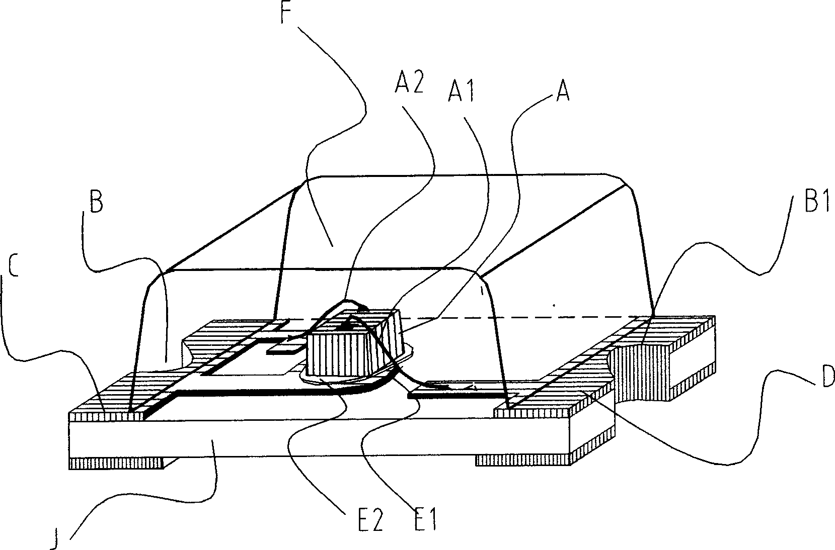
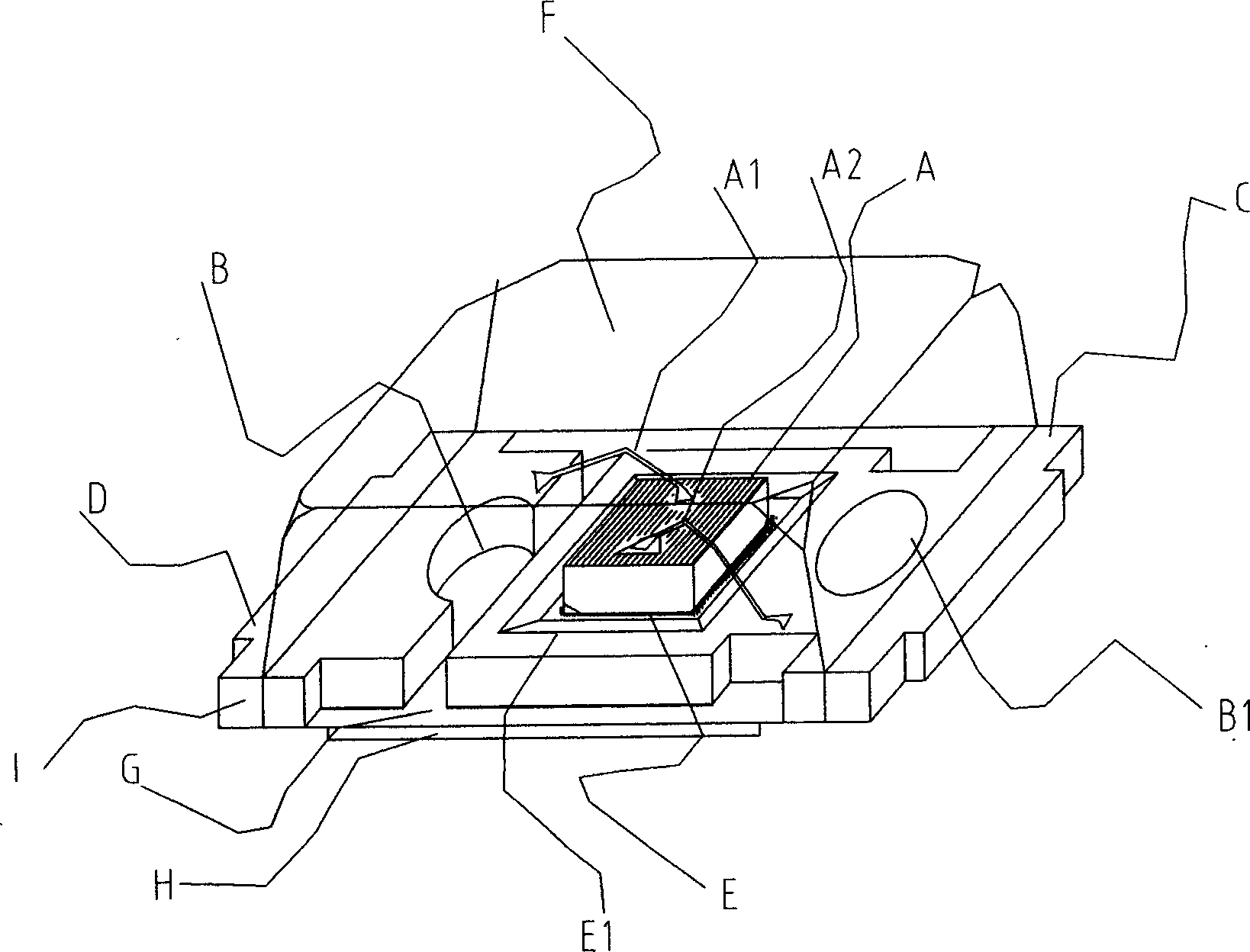
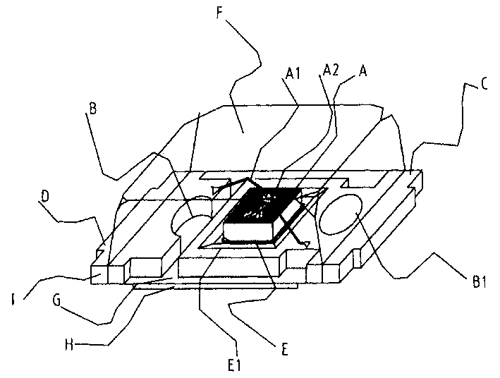
[0028] Such as figure 2 Shown, what the chip LED photo-semiconductor device of ultra-miniature of the present invention, ultrathin type is by anode lead frame (Anode Lead Frame) (D), negative electrode lead frame ((Dathode LeadFramed) (C), positive, negative electrode lead frame (D) Gold wires (A1) (A2) for conducting electricity between (C) and light-emitting chips (A), light-transmitting epoxy resin (F) for encapsulating the above two lead frames (D) (C), Lead The 10-50um protruding lower epoxy resin (H) formed on the lower end and the positive electrode lead through hole (B1) connecting Lead Frame, CathodeLead and the lower epoxy resin (H) to the upper epoxy resin (G), and the negative electrode lead through hole Hole (B2) constitutes.
PUM
 Abstract
Description
Claims
Application Information