Manufacturing method of semiconductor device
A manufacturing method and semiconductor technology, applied in semiconductor/solid-state device manufacturing, semiconductor devices, transistors, etc., can solve problems such as difficulty in forming overlaps
- Summary
- Abstract
- Description
- Claims
- Application Information
AI Technical Summary
Problems solved by technology
Method used
Image

Examples
Embodiment 1
[0033] In this embodiment, a case where a BPSG mold is used as an ion implantation mask instead of a protective film layer will be described.
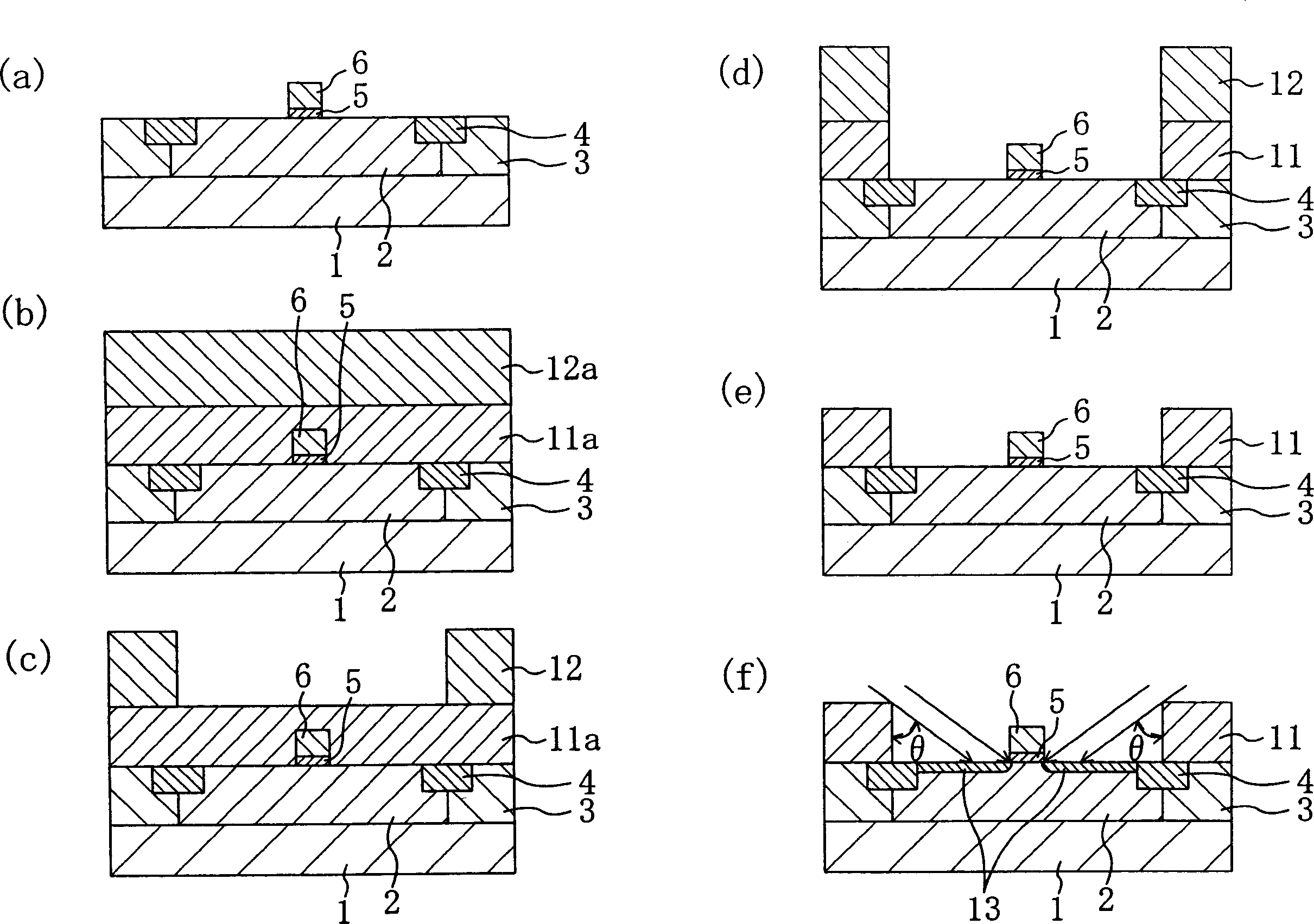
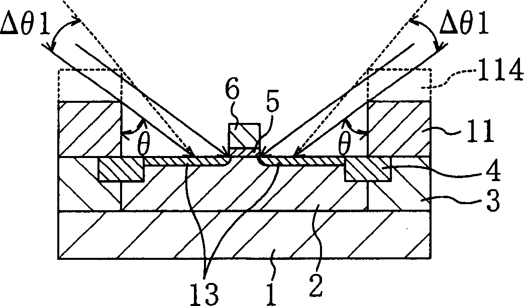
[0034] figure 1 (a) to (f) are the n steps from the manufacturing process of the semiconductor device of the first embodiment to the formation of the LDD structure. - Schematic cross-sectional view up to the layer process.
[0035] First, in figure 1 In the process shown in (a), a p-type region 2 with a width of 0.5 μm and an n-type region 3 located on the side of the p-type region 2 are formed on the upper part of the silicon substrate 1, and the p-type region 2 and the n-type region 3 are formed. Insulation film 4 is used for element isolation.
[0036] Then, a gate insulating film 5 having a thickness of 5 nm was formed on the p-type region 2 of the silicon substrate 1 by thermal oxidation. Then, a polysilicon film (not shown) is formed on the gate insulating film 5 by CVD, and a protective film (not shown) is formed on the poly...
Embodiment 2
[0046] In this embodiment, a case where a BPSG film having corners rounded by an etching process is used as an ion implantation mask will be described.
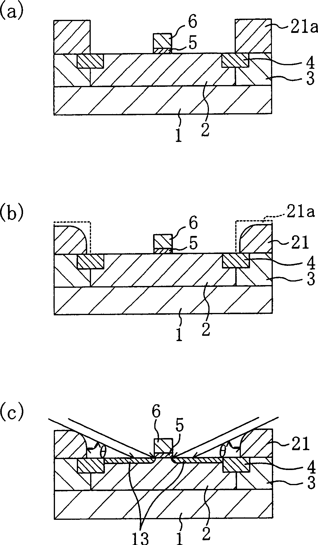
[0047] image 3 (a) to (c) are n steps from the manufacturing process of the semiconductor device of the embodiment to the formation of the LDD structure. - Schematic cross-sectional view up to the layer process.
[0048] First, in image 3 In the process shown in (a), in the same manner as in Example 1, a p-type region 2 and an n-type region 3 with a width of 0.5 μm are formed on the upper portion of the silicon substrate 1, and a p-type region 2 and an n-type region 3 are provided. Insulation film 4 is used for element isolation. Then, a gate insulating film 5 with a thickness of 5 nm and a gate electrode 6 with a gate length of 0.15 μm and a thickness of 0.2 μm were formed on the p-type region 2 . Then, the upper surface of p-type region 2 in silicon substrate 1 is opened, and hard mask 21a covering the region from the...
Embodiment 3
[0055] In Example 3, a BPSG film having corners rounded by a heat treatment process is used as an ion implantation mask.
[0056] Figure 5 (a) to (c) are the steps from n to the formation of the LDD structure in the manufacturing process of the semiconductor device of the third embodiment. - Schematic cross-sectional view up to the layer process.
[0057] First, in Figure 5 In the step shown in (a), p-type region 2 , n-type region 3 , and insulating film 4 for element isolation were formed on the upper portion of silicon substrate 1 in the same manner as in Example 1. Then, a gate insulating film 5 with a thickness of 5 nm and a gate electrode 6 with a gate length of 0.15 μm and a thickness of 0.2 μm were formed on the p-type region 2 . Then, a hard mask 31 a is formed on the upper surface of the p-type region 2 in the silicon substrate 1 to cover the region from the upper surface of the n-type region 3 through the upper surface of the insulating film 4 for element isolat...
PUM
 Abstract
Description
Claims
Application Information
 - R&D
- Intellectual Property
- Life Sciences
- Materials
- Tech Scout
- Unparalleled Data Quality
- Higher Quality Content
- 60% Fewer Hallucinations
Browse by: Latest US Patents, China's latest patents, Technical Efficacy Thesaurus, Application Domain, Technology Topic, Popular Technical Reports.
© 2025 PatSnap. All rights reserved.Legal|Privacy policy|Modern Slavery Act Transparency Statement|Sitemap|About US| Contact US: help@patsnap.com