Method for selective metal film layer removal using carbon dioxide jet spray

A metal film layer, high pressure carbon dioxide technology, used in semiconductor devices, electrical components, circuits, etc., can solve problems such as damage to metal conductors, and achieve the effect of accelerating solvent absorption

Inactive Publication Date: 2004-06-02
RAVE N P
View PDF1 Cites 12 Cited by
  • Summary
  • Abstract
  • Description
  • Claims
  • Application Information

AI Technical Summary

Problems solved by technology

The method proposed by Hayashi may be suitable for removing the baked photoresist template from the surface of the substrate, however, the carbon dioxide particle bombardment method proposed by Hayashi may greatly damage the metal conductor part, because depending on the nature of the force and friction, the method may not be able to avoid Conductor parts that do not need to be removed are removed

Method used


Image

  • Method for selective metal film layer removal using carbon dioxide jet spray
  • Method for selective metal film layer removal using carbon dioxide jet spray
  • Method for selective metal film layer removal using carbon dioxide jet spray

Examples


Embodiment Construction

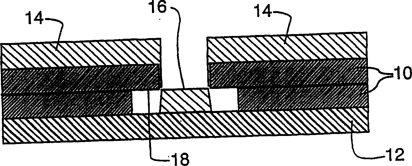
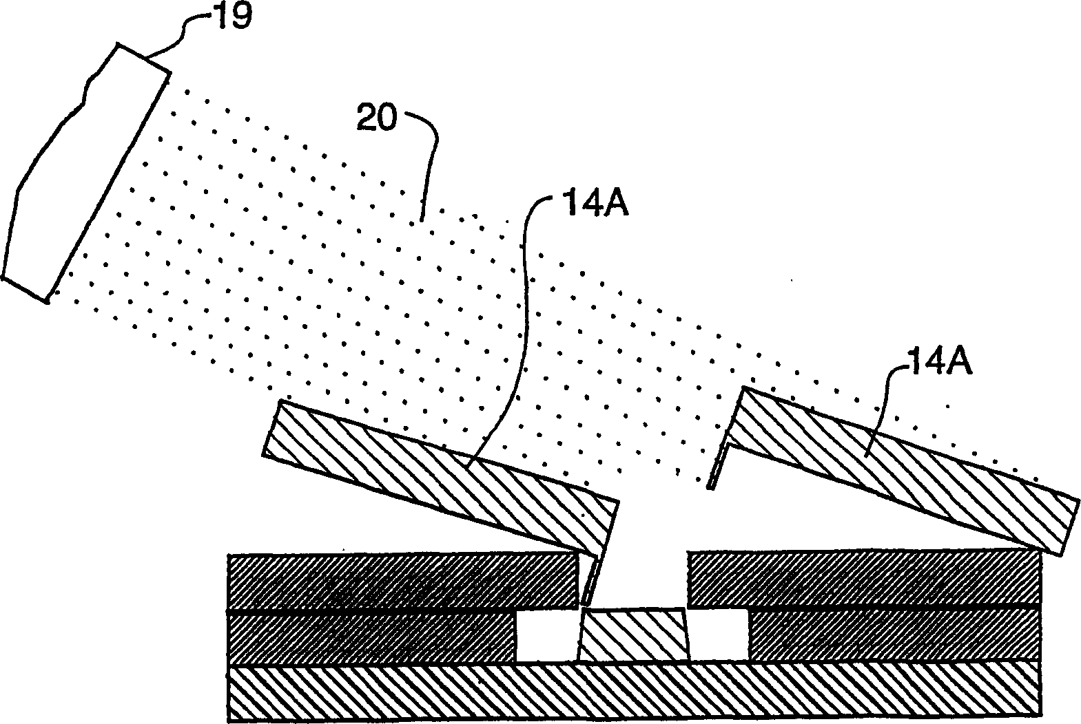
[0025] figure 1 A typical wafer to which a typical lift-off process has been applied to form a patterned conductor layer is shown. During this lift-off process, at least one layer of photoresist material 10 is deposited on the portion of wafer substrate 12 free of conductive material. The photoresist is exposed and developed in the following manner: Once the metal film material is deposited over the entire substrate surface in the metallization step, the metal film layer 14 deposited on the photoresist layer is separated from the metal conductor portion 16 deposited directly on the substrate. will be discontinuous. This allows subsequent removal of the metal film layer 14 on the photoresist, leaving the metal conductor 16 intact on the substrate, as desired by the patterning process.

[0026] The discontinuity between the metal conductor portion 16 and the metal layer 14 is preferably achieved by applying a layer of photoresist such that the sidewalls 18 of the photoresist d...


PUM


Abstract

A method for the selective removal of the metal film layer (14) accumulated upon a photoresist layer (10) during processing of substrates using a stream of carbon dioxide spray (20) without disturbing conductor portions is provided. A constant stream (20) of high pressure CO2 snow is applied to the metal film layer thereby rapidly cooling the metal layer on top of said resist layer causing it to shrink rapidly, and to debond, and peel from the photoresist layer underneath. The temperature of the substrate is raised and maintained at significantly higher than room temperature. Continuing the application of the CO2 spray causes thermal shock to the photoresist under the metalized layer causing large cracks in the remaining metal layer portions, said cracks typically including at least one loose metal edge. The CO2 spray is continually applied to the cracks thereby peeling away the remaining metal portions, leaving the exposed photoresist and underlying surface features. Preferably, continued treatment of the surface with CO2 snow particals erodes a surface layer of the photoresist and heavily cross-linked layers created during the metalization process. After the metal layer and the surface layer of the photoresist are removed, a simple chemical strip, such as acetone, completely removes all the remaining resist, leaving the wafer with undamaged conductor portions.

Description

technical field [0001] The present invention relates to a method for selectively removing metal film layers accumulated during "lift off" of substrates such as wafers, integrated circuits, masks, etc., using a carbon dioxide spray stream. Background technique [0002] A common method of forming a patterned conductor layer on a substrate during the fabrication of integrated circuits, among other processes, is a process that typically involves depositing a layer of photoresist onto the patterned substrate so that the photolithographic The glue covers the portion of the substrate that is not coated with conductive material. The photoresist layer is usually exposed and developed so that when the metal layer covers the entire surface, the portion of the metal layer deposited on top of the photoresist layer is discontinuous from the metal layer (conductor portion) deposited directly on the substrate . Such discontinuities are typically obtained by developing patterned sidewalls ...

Claims


Application Information

Patent Timeline
Patent Type & Authority Applications(China)
IPC IPC(8): H01L21/28H01L21/3065H01L21/3213
CPCH01L21/32131
Inventor C·W·鲍尔斯
Owner RAVE N P
Why Eureka
Try Eureka