Semiconductor device

A semiconductor and device technology, applied in the field of electrical short-circuited semiconductor devices, to achieve the effect of preventing electrical short-circuits

Inactive Publication Date: 2004-08-25
RENESAS TECH CORP
View PDF2 Cites 4 Cited by
  • Summary
  • Abstract
  • Description
  • Claims
  • Application Information

AI Technical Summary

Problems solved by technology

[0007] However, in the manufacturing method of the above-mentioned semiconductor device, there is a problem that an additional process for removing the conductive film located in the dicing line region must be provided in the state of the wafer.

Method used


Image

  • Semiconductor device
  • Semiconductor device
  • Semiconductor device

Examples


Embodiment 1

[0029] A method of manufacturing a semiconductor device according to Embodiment 1 of the present invention and a semiconductor device manufactured by the method will now be described.

[0030] First, processing to be performed in the state of the wafer for forming predetermined elements, wiring, and the like on the wafer is completed. At this time, in the dicing line region of the wafer, the conductive film for forming wiring and the like remains without being removed.

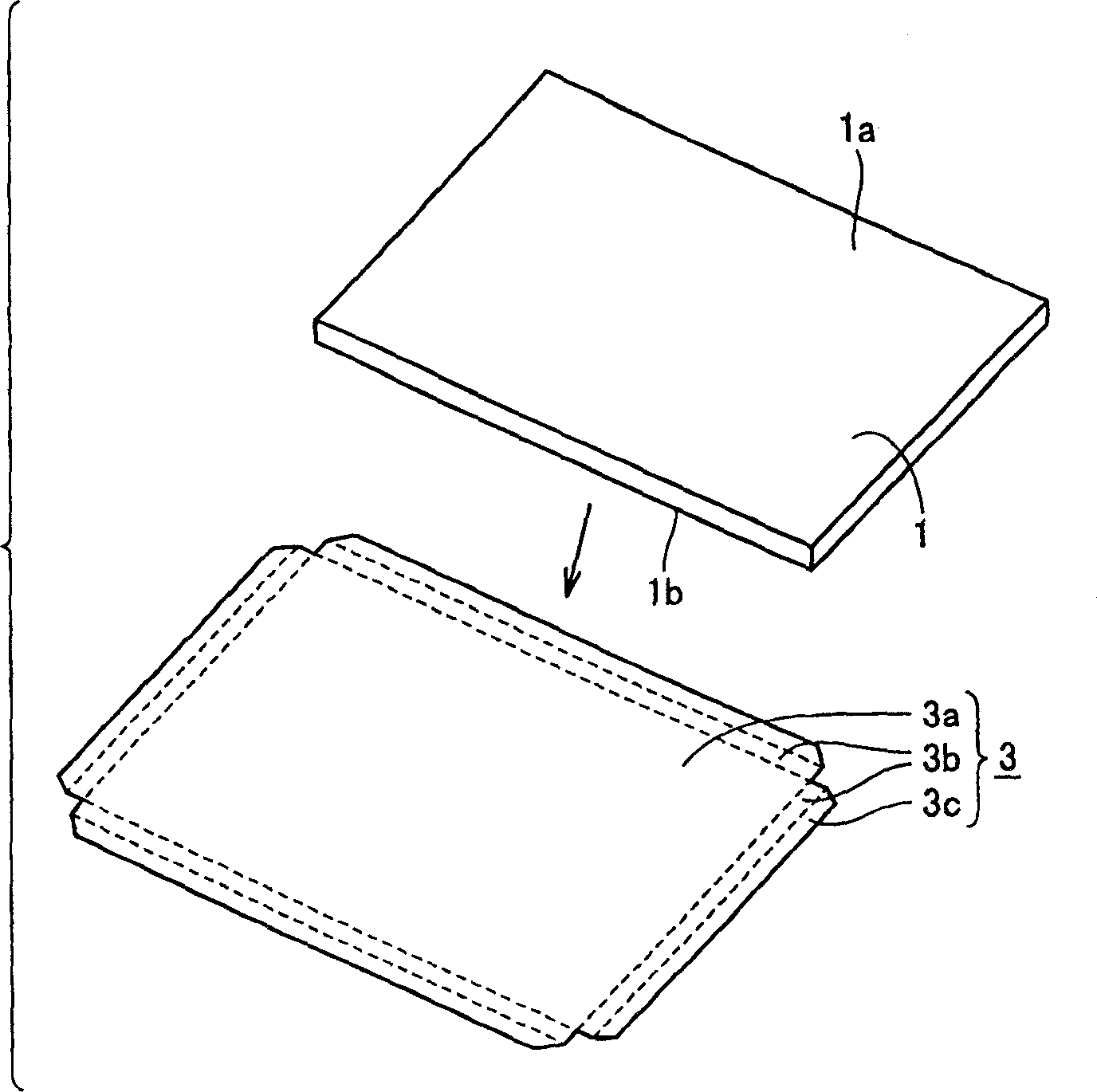
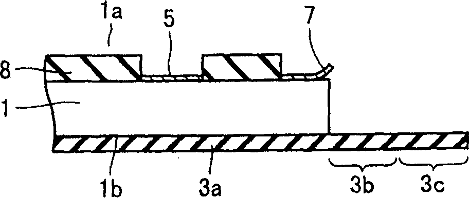
[0031] By dicing the wafer, such as figure 1 As shown, the semiconductor chip 1 is cut out. Such as figure 2 As shown, the surface 1a of the semiconductor chip 1 is covered with the passivation film 8, and the electrode portion 5, which is a so-called bonding pad, is exposed at the portion where the bonding wire is connected.

[0032] In addition, in the peripheral portion of the semiconductor chip 1 , there is a portion (burr) 7 rolled up by dicing in the conductive film remaining in the region of the dic...

Embodiment 2

[0045] A method of manufacturing a semiconductor device according to Embodiment 2 of the present invention and a semiconductor device manufactured by this method will now be described.

[0046] First, if Figure 8 As shown, in the same manner as the above-mentioned manufacturing method, dicing is performed in the dicing line region of the wafer without removing the conductive film for forming wiring and the like, leaving the semiconductor chip 1 out.

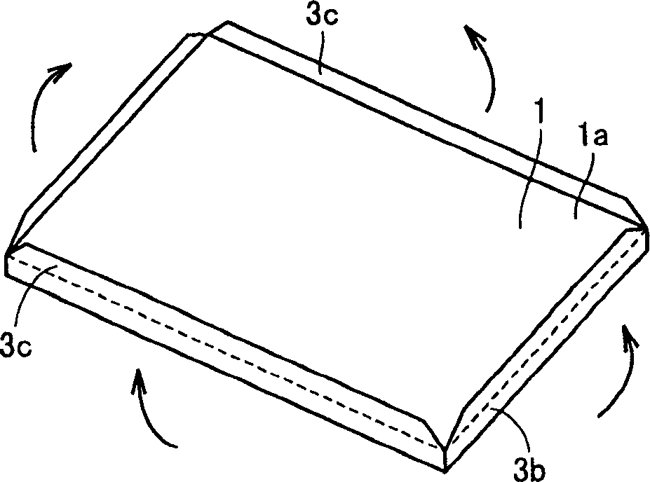
[0047] Then, if Figure 8 As shown, the insulating sheet member 3 attached to the semiconductor chip 1 is prepared so as to cover a predetermined portion of the semiconductor chip 1 . As the material of the insulating sheet member 3, a resin sheet member or a rubber sheet member can be used, and as will be described later, it is preferable to melt it by soldering heat in wire bonding.

[0048] At this time, the insulating sheet member 3 is provided with a first sticking portion 3a sticking to the surface 1a of the semiconducto...


PUM


Abstract

A semiconductor chip is produced through dicing without removing a conductive film for forming an interconnection and the like from a dicing line region. A prescribed insulating sheet member is adhered to this semiconductor chip at its back face, and the back face and the side face of semiconductor chip, and part of a front face along the periphery of semiconductor chip are covered by insulating sheet member. Thus, even when the conductive film in the dicing line region is curled up by dicing and a burr is resulted at the periphery of semiconductor chip, burr is covered by insulating sheet member to prevent a wire and burr from directly contacting to each other. Thus, a semiconductor device in which an electrical short circuit is prevented without removing a conductive film from a dicing line can be obtained.

Description

technical field [0001] The present invention relates to a semiconductor device, in particular to a semiconductor device which prevents electrical short circuit between burr and welding wire which occurs during cutting. Background technique [0002] In the manufacture of semiconductor devices, first, elements, wiring, and the like are formed by subjecting the surface of the wafer to a predetermined process in the state of a semiconductor substrate (wafer). Once all the processing to be carried out in the state of the wafer has been completed, the wafer is diced along dicing lines, and individual semiconductor chips are cut out. [0003] A predetermined packaging process including a predetermined die bonding process and a wire bonding process is performed on each of the cut out semiconductor chips to complete a semiconductor device. [0004] However, if the wafer is diced along the dicing line, the conductive film in the area of ​​the dicing line is rolled up. Therefore, whe...

Claims


Application Information

Patent Timeline
Patent Type & Authority Applications(China)
IPC IPC(8): H01L21/60H01L21/301H01L23/31
CPCH01L23/3185H01L24/48H01L24/85H01L24/45H01L2924/01082H01L2924/0105H01L2924/00014H01L2224/85399H01L2924/01004H01L24/05H01L2224/48463H01L2924/01068H01L2224/45099H01L2224/04042H01L23/3164H01L2924/01005H01L2924/01033H01L2924/01006H01L2224/05599H01L2224/4847H01L2224/85009H01L2224/05556H01L2924/014H01L21/30
Inventor 德光成太清水悟
Owner RENESAS TECH CORP
Why Eureka
Try Eureka