Electronic device manufacturing method

A technology of electronic devices and manufacturing methods, which is applied in semiconductor/solid-state device manufacturing, electrical components, circuits, etc., can solve problems such as wiring patterns cannot be normally resolved, resist poisoning, etc., to expand the range of structure selection, prevent Resist poisoning phenomenon, effect of reducing variation in film thickness

Inactive Publication Date: 2004-08-25
RENESAS ELECTRONICS CORP +1
View PDF1 Cites 6 Cited by
  • Summary
  • Abstract
  • Description
  • Claims
  • Application Information

AI Technical Summary

Problems solved by technology

[0006] A chemically amplified resist has a structure in which hydrogen ions are generated by exposure to light and used as a catalyst to thermally react the resist resin to resolve patterns. However, in the case of using such a chemically amplified resist, the On the hole pattern, especially on the isolated hole pattern and the wiring pattern on the outermost hole of the densely arranged hole pattern, the normal resolution may not be possible, which may cause the phenomenon of so-called resist poisoning.

Method used


Image

  • Electronic device manufacturing method
  • Electronic device manufacturing method
  • Electronic device manufacturing method

Examples


Embodiment Construction
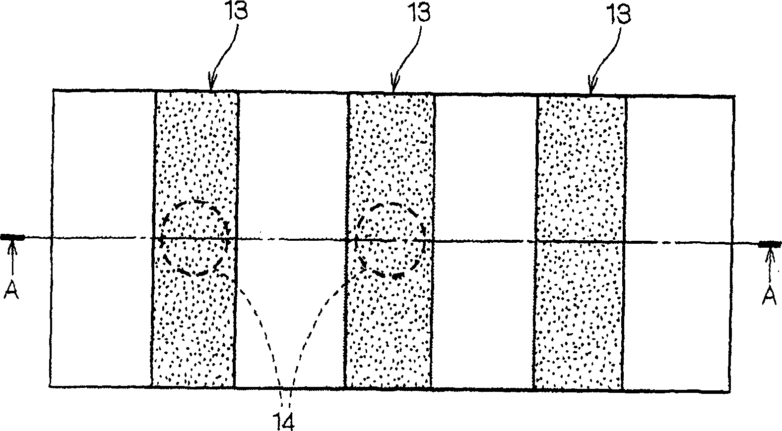
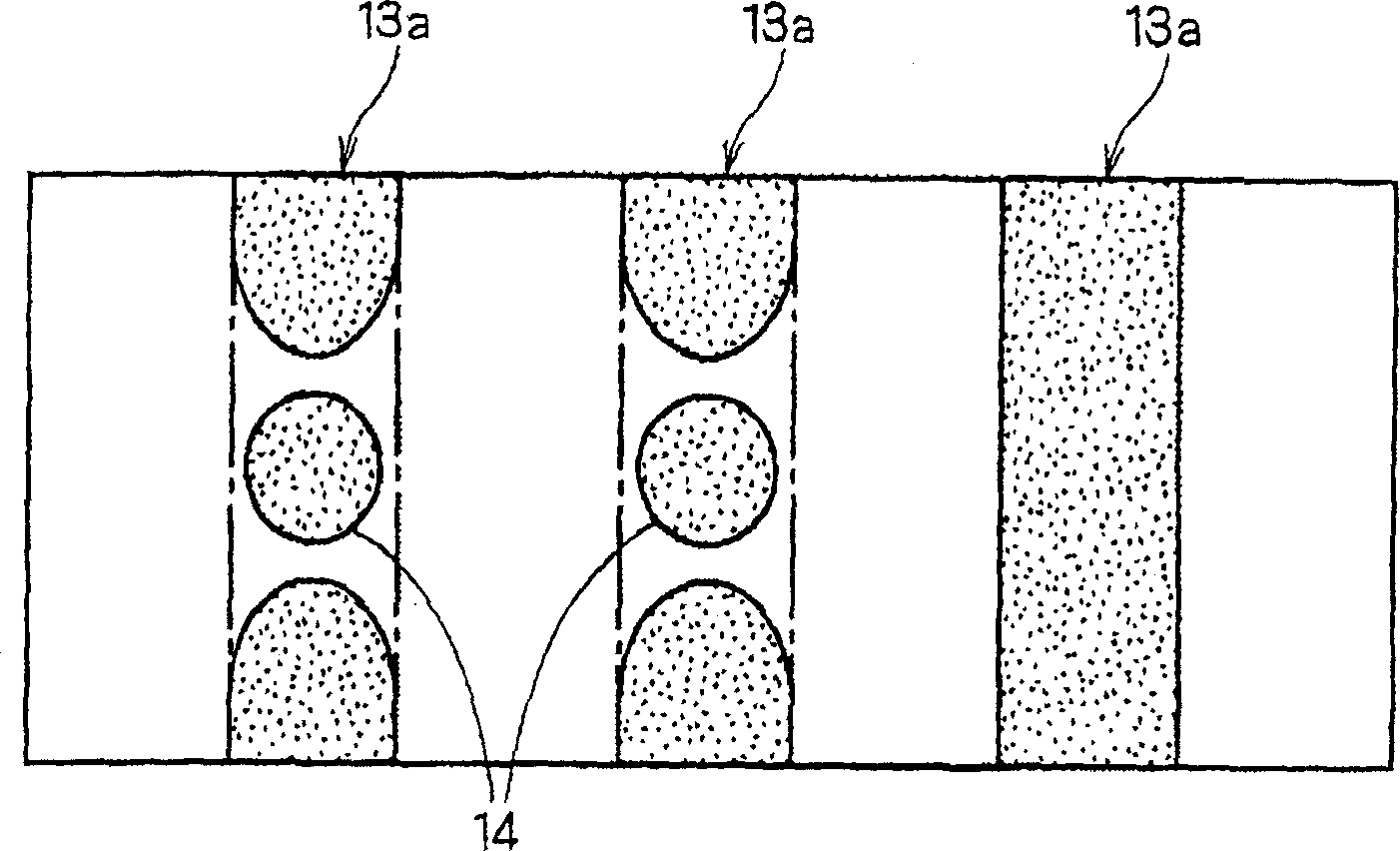
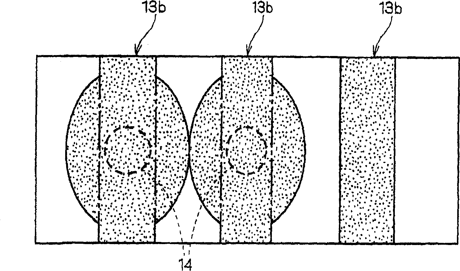
[0043]

[0044] Before describing the embodiment of the invention, the phenomenon of resist poisoning will be further explained.

[0045] In most cases, a semiconductor device having a buried multilayer wiring structure has an etching stopper film between an interlayer insulating film and an underlying structure, and an upper layer on the interlayer insulating film. protective film. At the same time, in order to suppress the increase in parasitic capacitance accompanying the adoption of a multilayer structure and enable high-speed operation, as an interlayer insulating film, carbon is introduced into silicon oxide in most cases, and the density is lower than that of general silicon oxide. , A low dielectric constant interlayer insulating film with a low dielectric constant.

[0046] In such a structure, when the upper protective film is formed, on the interface between the upper protective film and the low-permittivity interlayer insulating film, the surface decomposition a...


PUM

PropertyMeasurementUnit
thicknessaaaaaaaaaa
thicknessaaaaaaaaaa
thicknessaaaaaaaaaa

Abstract

It is an object to provide a semiconductor device having a buried multilayer wiring structure in which generation of a resolution defect of a resist pattern is suppressed and generation of a defective wiring caused by the resolution defect is reduced. After a via hole (7) reaching an etching stopper film (4) is formed, annealing is carried out at 300 to 400 DEG C. with the via hole (7) opened. As an annealing method, it is possible to use both a method using a hot plate and a method using a heat treating furnace. In order to suppress an influence on a lower wiring (20) which has been manufactured, heating is carried out for a short time of approximately 5 to 10 minutes by using the hot plate. Consequently, a by-product staying in an interface of an upper protective film (6) and an interlayer dielectric film (5) having a low dielectric constant and a by-product staying in an interface of the etching stopper film (4) and the interlayer dielectric film (5) having a low dielectric constant are discharged so that an amount of the residual by-product can be decreased.

Description

technical field [0001] The present invention relates to a method of manufacturing an electronic device, in particular to a method of manufacturing an electronic device having a buried multilayer wiring structure. Background technique [0002] In the manufacturing method of a semiconductor device having a buried multilayer wiring structure, recently, in order to electrically connect the structure of the bottom layer arranged with an interlayer insulating film interposed therebetween and the upper layer wiring, a so-called double wiring method is used. Heavy metal mosaic (dual-damascene) method. This method is a method of simultaneously forming a plug penetrating an interlayer insulating film to reach a lower layer structure, and an upper layer wiring, and an example thereof is disclosed in Patent Document 1. [0003] That is, in Patent Document 1, a resist material is filled in a contact hole penetrating an interlayer insulating film to reach a semiconductor substrate, and t...

Claims


Application Information

Patent Timeline
Patent Type & Authority Applications(China)
IPC IPC(8): H01K3/10H01L21/768H05K3/10
CPCH01L21/76808Y10T29/49117Y10T29/49126Y10T29/4913Y10T29/49144Y10T29/49155Y10T29/49165H01L21/768
Inventor 西冈康隆坂井淳二郎友久伸吾松本晋岩本文男山中通成
Owner RENESAS ELECTRONICS CORP
Why Eureka
Try Eureka