Making process of pattern on wafer and its application
A manufacturing method and wafer technology, which are applied in the field of pattern making on wafers, can solve the problems of difficult process control, low production efficiency, cracks and the like, and achieve the effects of simple equipment, low cost and low investment.
- Summary
- Abstract
- Description
- Claims
- Application Information
AI Technical Summary
Problems solved by technology
Method used
Image
Examples
Embodiment 1
[0021] Embodiment 1 adopts light-transmitting good glass to make a disc with a central hole, the size of which is consistent with that of a 120mm disc, and then coats the glass disc with photosensitive adhesive to make a recordable disc; Record the pattern that needs to be etched on the silicon dioxide film on the wafer. The light source in the disc recorder is a laser with a wavelength of 650nm; then develop the patterned glass disc to make a mask plate; the same method produces metal aluminum wiring Reticle. Then put the glass wafer mask plate corresponding to the etching pattern of the silicon dioxide film layer on the silicon wafer coated with photosensitive adhesive through oxidation, and use the light source to irradiate and expose the area determined by the mask plate, and then place the silicon wafer on the Develop in the developer; then etch the silicon wafer, and then remove the hardened photoresist on the silicon wafer; vapor-deposit a layer of metal aluminum on the...
Embodiment 2
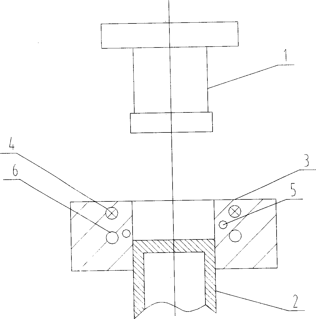
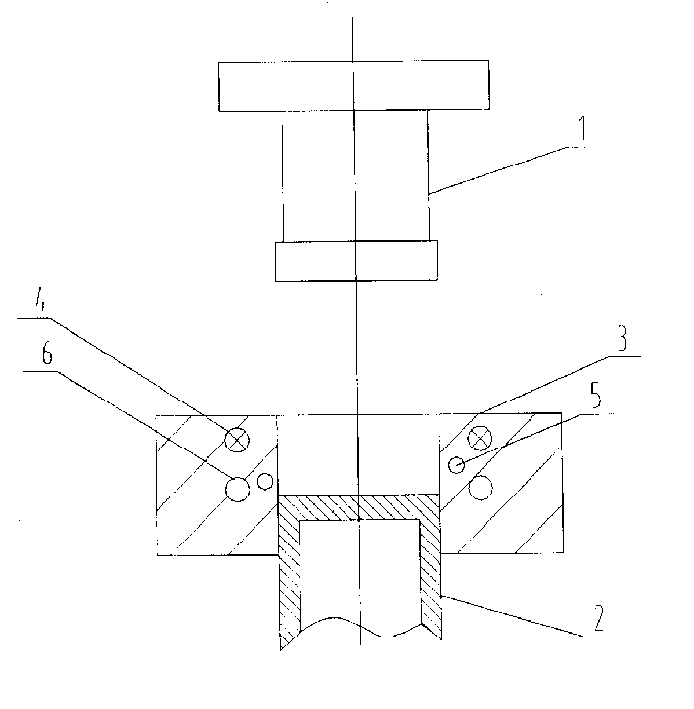
[0023] first use figure 1 The mold shown is used to shape the desired silicon wafer. Such as figure 1 As shown, the male mold 1 and the male mold 2 are placed in the female mold 3, and the heating element 4 is energized to preheat the mold, and the thermocouple 5 can collect the temperature on the female mold 3. After reaching the set temperature, the male mold 1 is removed from the The female mold 3 exits upwards, and the male mold 2 stays at the bottom of the female mold 3. Liquid silicon is poured into the female mold 3. The superheated temperature of the liquid silicon is 1500°C, and it will not solidify immediately when poured into the female mold 3. The positive mold 1 is then pressed against the liquid silicon. According to the temperature collected by the temperature acquisition sensor, it is judged whether to pass water through the cooling pipe 6 to cool the female mold 3 or to energize the heating element 4 to heat the female mold 3, so as to ensure that the liquid...
PUM
 Abstract
Description
Claims
Application Information
 - R&D
- Intellectual Property
- Life Sciences
- Materials
- Tech Scout
- Unparalleled Data Quality
- Higher Quality Content
- 60% Fewer Hallucinations
Browse by: Latest US Patents, China's latest patents, Technical Efficacy Thesaurus, Application Domain, Technology Topic, Popular Technical Reports.
© 2025 PatSnap. All rights reserved.Legal|Privacy policy|Modern Slavery Act Transparency Statement|Sitemap|About US| Contact US: help@patsnap.com


