

Electronic beam focusing equipment and electronic beam projection micro shadow system using the same equipment
A technology of focusing equipment and electron beams, which is applied in the direction of optomechanical equipment, microlithography exposure equipment, nanotechnology for information processing, etc., can solve the problem of difficulty in forming patterns with nanometer-scale line widths, increased manufacturing costs, and inability to problems such as uniformity
- Summary
- Abstract
- Description
- Claims
- Application Information
AI Technical Summary
Problems solved by technology
Method used
Image

Examples
Embodiment Construction
[0025] An electron beam focusing apparatus and an electron beam projection lithography (EPL) system according to preferred embodiments of the present invention will be described below with reference to the accompanying drawings. The same reference numerals in different figures represent the same components.
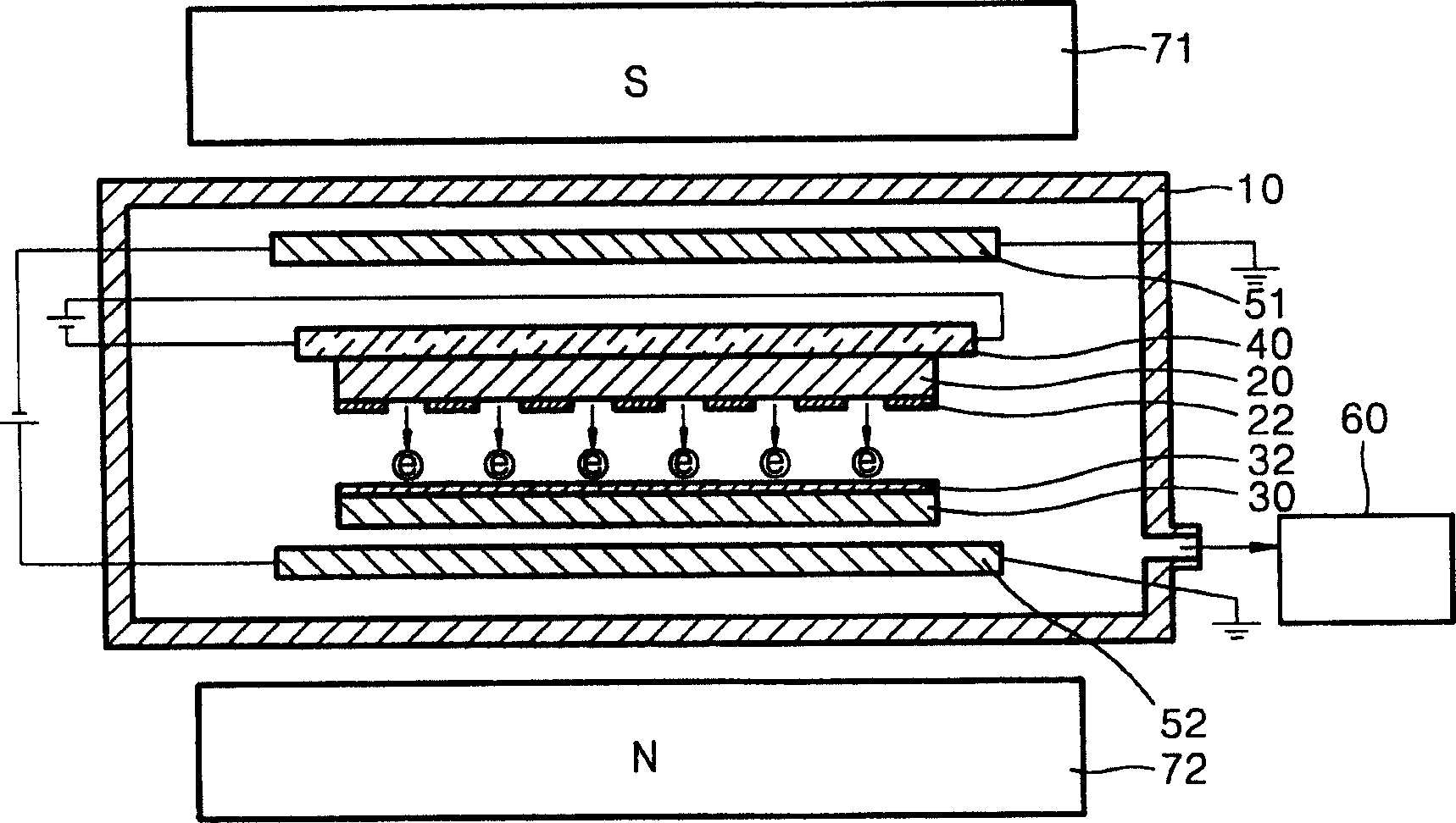
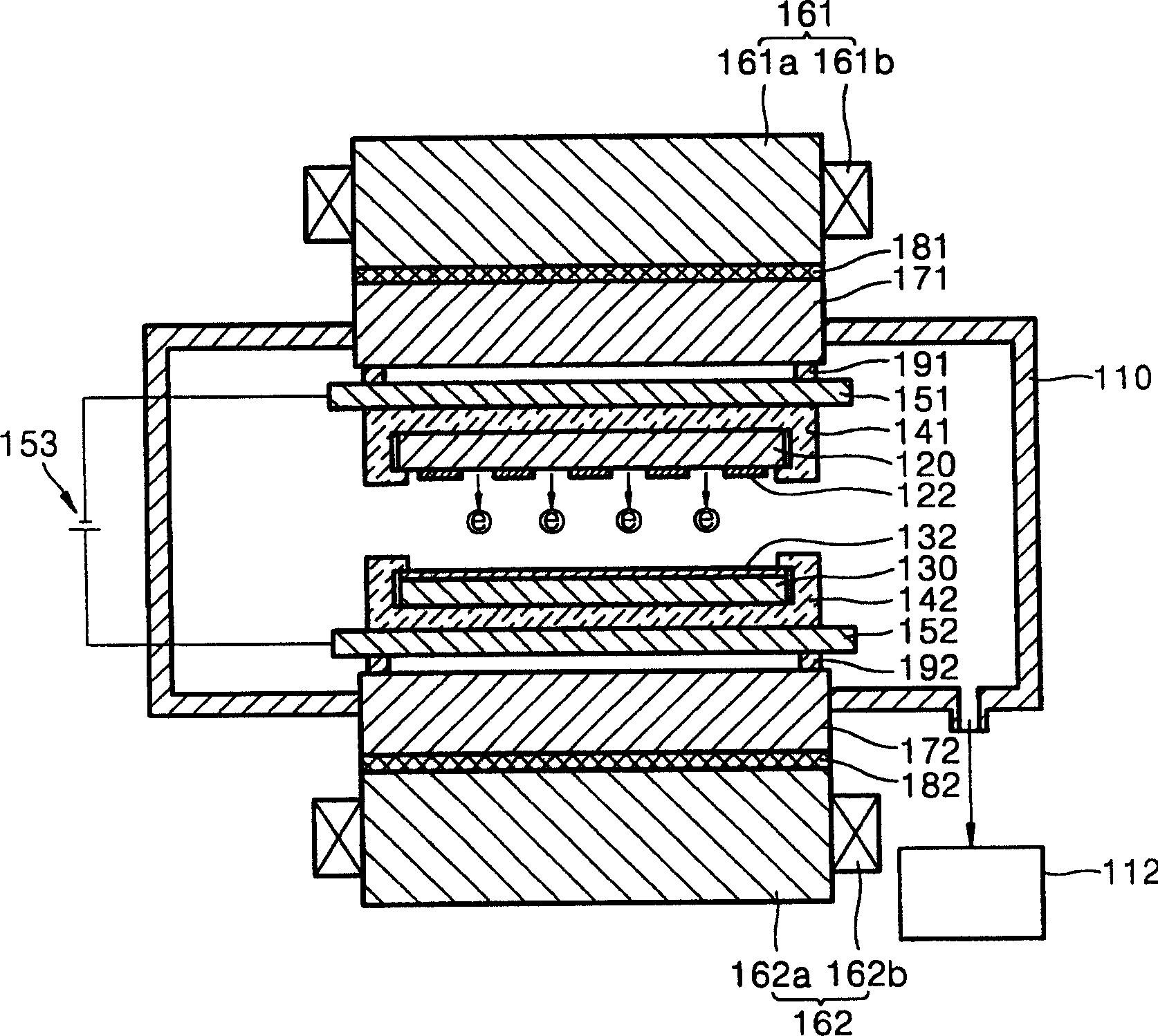
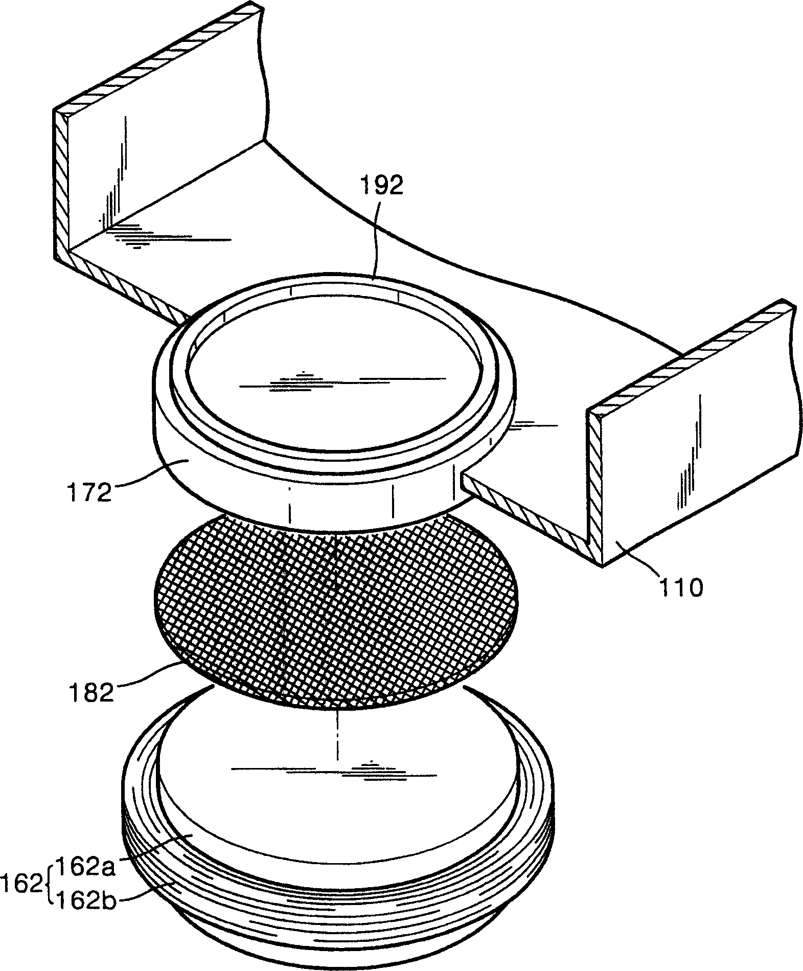
[0026] see figure 2 and image 3 , as the EPL system of the present invention comprises: a vacuum chamber 110, it surrounds a space, and a wafer 130 is placed wherein; An electron beam emitter 120, is installed in the vacuum chamber 110; 120 electron beam focusing devices in the path of the emitted electron beam.
[0027] The vacuum chamber 110 is connected to a vacuum pump 112 to maintain a vacuum in the vacuum chamber. In this case, the vacuum chamber is preferably made of non-magnetic material. This can prevent the magnetic flux generated by the top and bottom magnets 161 and 162 from leaking out of the vacuum chamber 110 as described later. The vacuum chamber ca...
PUM
 Abstract
Description
Claims
Application Information