Saphire base nitride chip scribing method

A sapphire and nitride technology, applied in the dicing field of sapphire-based nitride chips, can solve the problems of low laser absorption, unfavorable laser dicing efficiency, and influence on the optoelectronic properties of GaN/sapphire LED chips, so as to improve production efficiency and ensure The effect of optoelectronic properties

Inactive Publication Date: 2004-09-15
SHANGHAI INST OF OPTICS & FINE MECHANICS CHINESE ACAD OF SCI
View PDF1 Cites 10 Cited by
  • Summary
  • Abstract
  • Description
  • Claims
  • Application Information

AI Technical Summary

Problems solved by technology

[0003] However, there are also problems with laser scribing technology: (1) Since sapphire is a transparent medium, its absorption of laser light is very small, which is not con

Method used


Image

  • Saphire base nitride chip scribing method
  • Saphire base nitride chip scribing method

Examples


Embodiment Construction

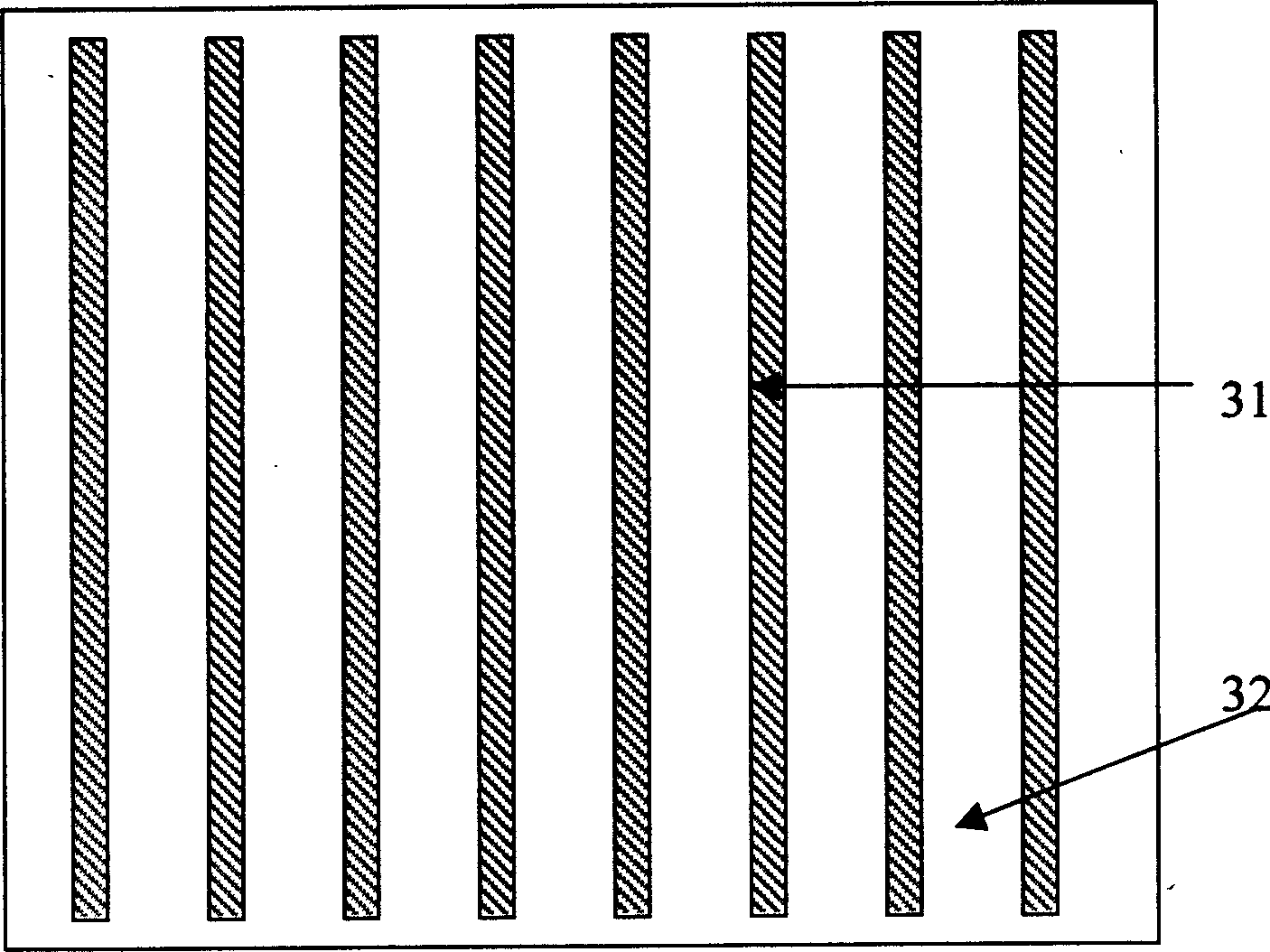
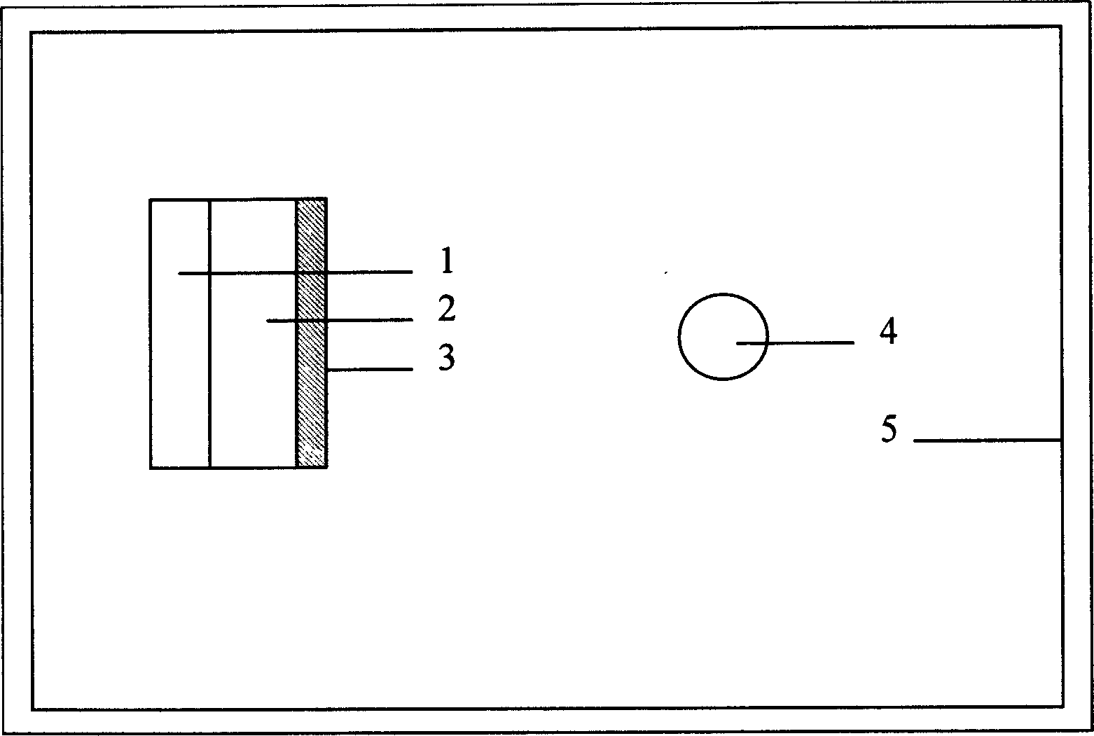
[0022] see first figure 1 and figure 2 , figure 1 and figure 2 They are the schematic diagram of the irradiation baffle and the schematic diagram of the irradiation device according to the embodiment of the present invention, respectively.

[0023] The scribing method of the sapphire-based nitride chip in the embodiment of the present invention is characterized in that it includes the following steps:

[0024] According to the size of the chip to be scribed, a 300×300×3mm irradiation baffle 3 is made of a lead plate. The size of the baffle is the same as that of the chip. The width of the slit 31 in the baffle is about 0.2mm. The slit spacing 32 is 35nm, and the thickness of the baffle is about 3-10mm, see figure 1 ;

[0025] The back side of the sapphire substrate 2 that has grown GaN is closely attached to the radiation baffle 3, and the Co 60 The irradiation source 4 performs Gamma ray irradiation in the irradiation room 5, and the irradiation dose is 10 8 Rad; ...


PUM

PropertyMeasurementUnit
Wavelengthaaaaaaaaaa

Abstract

The method includes following steps: based on scribing requirement, using lead plate makes irradiation baffle with several slots in middle; adhibiting rear face of sapphire crystal with GaN being developed on the irradiation baffle closely, carrying out irradiation of Gamma ray by using Co60 in irradiation dose about 10 to the power 7 Rad; then, rotating baffle at 90 degree, carrying irradiation with same dose forms meshy irradiation lines on substrate of sapphire; scribing is carried out for exposured GaN/sapphire LED chip along irradiation line by using KrF quasi molecule laser in 248nm; splinting is carrier out for GaN/sapphire LED chip scribed by using splinter device, then testing chip through probe and sorting chips. Advantages of the invention are smooth edge, not affecting on photoelectric properties of GaN.

Description

Technical field: [0001] The invention relates to a scribing method for a sapphire-based nitride chip. Background technique: [0002] Due to the wide application of ultra-high brightness GaN / sapphire laser diode (LED) in indoor and outdoor color display, traffic signal indication, LED background light source and white lighting source, its production scale has expanded rapidly. In the production process, the GaN / sapphire LED chip cutting problem has become one of the important factors hindering the further reduction of its production cost. Since GaN / sapphire is much harder than ordinary compound semiconductor materials such as GaAs and GaP, when cutting with a grinding wheel tool, the amount of tool wear is extremely large, and the amount of cut is also small. Generally, diamond cutters are used to cut GaN / sapphire LED chips, and the cutting is generally divided into two steps: scribing and splitting: first, use a device equipped with a diamond cutter to scribe according to t...

Claims


Application Information

Patent Timeline
IPC IPC(8): B23K26/38H01L21/301H01S5/00
Inventor 徐军蒋成勇周圣明杨卫桥周国清王银珍彭观良邹军刘士良张俊计邓佩珍
Owner SHANGHAI INST OF OPTICS & FINE MECHANICS CHINESE ACAD OF SCI
Why Eureka
Try Eureka