Manufacturing method of read only memory

A technology of read-only memory and manufacturing method, which is applied in semiconductor/solid-state device manufacturing, electrical components, circuits, etc., and can solve problems such as reliability of components, affecting the integrity of implanted contours, and poor distribution of implanted ions, etc., to achieve Good intrusion effect, good integrity effect

Inactive Publication Date: 2004-10-06
MACRONIX INT CO LTD
View PDF0 Cites 6 Cited by
  • Summary
  • Abstract
  • Description
  • Claims
  • Application Information

AI Technical Summary

Problems solved by technology

[0003] In the known Nitride ROM process, after etching to define the silicon oxide / silicon nitride / silicon oxide stack layer, ion implantation of buried drain (BD) is usually carried out However, the previous etching process will form or leave particles on the bottom or sidewall, and these particles are equivalent to a hard mask during the ion implantation process of the buried drain. As a result, the distribution of implanted ions is not good, and the integrity of the subsequently formed buried drain oxide is not good, which leads to reliability problems of the device
[0004] Moreover, for ROMs with floating gates, since the source / drain implantation process is usually performed after etching to define the gate structure, the problem of the aforementioned particles being implanted into a hard mask is also a problem. May occur, the result of which will also affect the integrity of the implant profile, thereby creating component reliability issues

Method used


Image

  • Manufacturing method of read only memory
  • Manufacturing method of read only memory
  • Manufacturing method of read only memory

Examples


Embodiment Construction

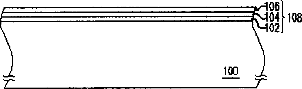
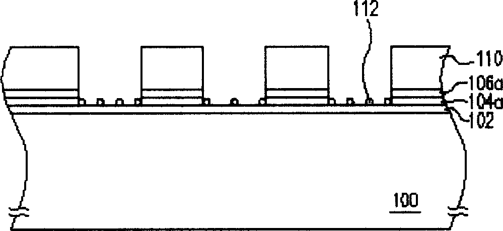
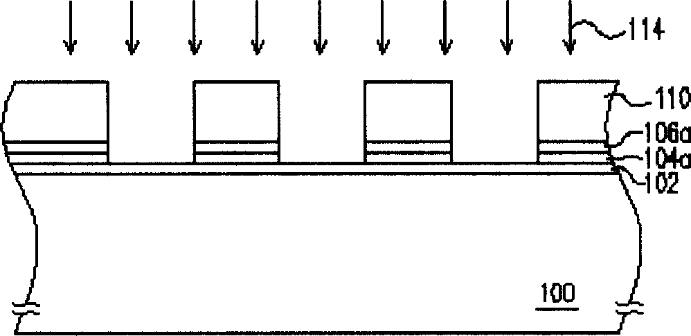
[0036] Figure 1A to Figure 1E Shown is a schematic cross-sectional view of a manufacturing process of a read-only memory according to a preferred embodiment of the present invention, and is suitable for manufacturing a silicon nitride read-only memory.

[0037] First, please refer to Figure 1A , deposit a silicon nitride stack layer 108 on the substrate 100, and the stack structure formed by it is, for example, a bottom oxide layer (bottom oxide layer) 102, a layer of silicon nitride layer 104 and a top oxide layer (top oxide layer). oxide layer) 106 composed of silicon oxide / silicon nitride / silicon oxide (ONO) composite layer. Wherein the bottom oxide layer 102 is formed by thermal oxidation, for example, the silicon nitride layer 106 is formed by chemical vapor deposition, and the top oxide layer 106 is formed by using wet hydrogen / oxygen (H 2 / O 2 gas) to oxidize part of the silicon nitride layer 104.

[0038] Next, please refer to Figure 1B , define the top oxide l...


PUM


Abstract

A process for preparing ROM includes generating silicon nitride stack on substrate, etching to define the silicon nitride stacks but retaining the oxidized bottom layer, washing, and ion transplantation for generating doped region in substrate between defined silicon nitride stack layers.

Description

technical field [0001] The present invention relates to a manufacturing method of a memory, and in particular to a manufacturing method of a read-only memory (Read Only Memory, ROM). Background technique [0002] In read-only memory, flash memory has the advantages of being programmable, erasable, and retaining data after power-off, and compared with erasable and programmable read-only memory, it has the advantages of in-circuit Due to the advantages of electrical programming and electrical removal, it has become a widely used read-only memory device in personal computers and electronic equipment. [0003] In the known Nitride ROM process, after etching to define the silicon oxide / silicon nitride / silicon oxide stack layer, ion implantation of buried drain (BD) is usually carried out However, the previous etching process will form or leave particles on the bottom or sidewall, and these particles are equivalent to a hard mask during the ion implantation process of the buried ...

Claims


Application Information

Patent Timeline
Patent Type & Authority Applications(China)
IPC IPC(8): H01L21/8246H01L21/8247
Inventor 刘振钦
Owner MACRONIX INT CO LTD
Why Eureka
Try Eureka