Comparator circuit and bias compensator

A technology for comparing circuits and compensating devices, which is applied in the fields of physical parameter compensation/prevention, electrical components, analog/digital conversion calibration/testing, etc., and can solve problems such as difficulties, increased occupied area of ​​semiconductor devices, and low power consumption.

Inactive Publication Date: 2004-10-27
PANASONIC CORP
View PDF0 Cites 17 Cited by
  • Summary
  • Abstract
  • Description
  • Claims
  • Application Information

AI Technical Summary

Problems solved by technology

However, in view of the fact that an increase in the occupied area of ​​a semiconductor device (IC) must be avoided, or that lower power consumption is required, it is actually very difficult to provide a specially designed circuit capable of adjusting the bias of the comparator. difficult

Method used


Image

  • Comparator circuit and bias compensator
  • Comparator circuit and bias compensator
  • Comparator circuit and bias compensator

Examples


no. 1 example

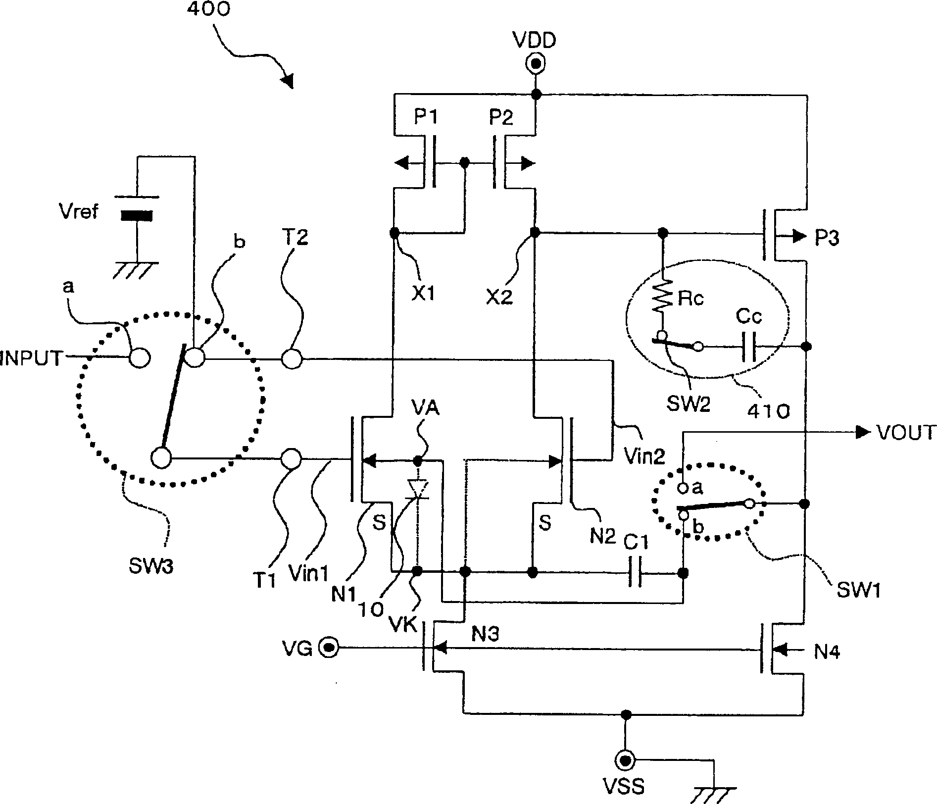
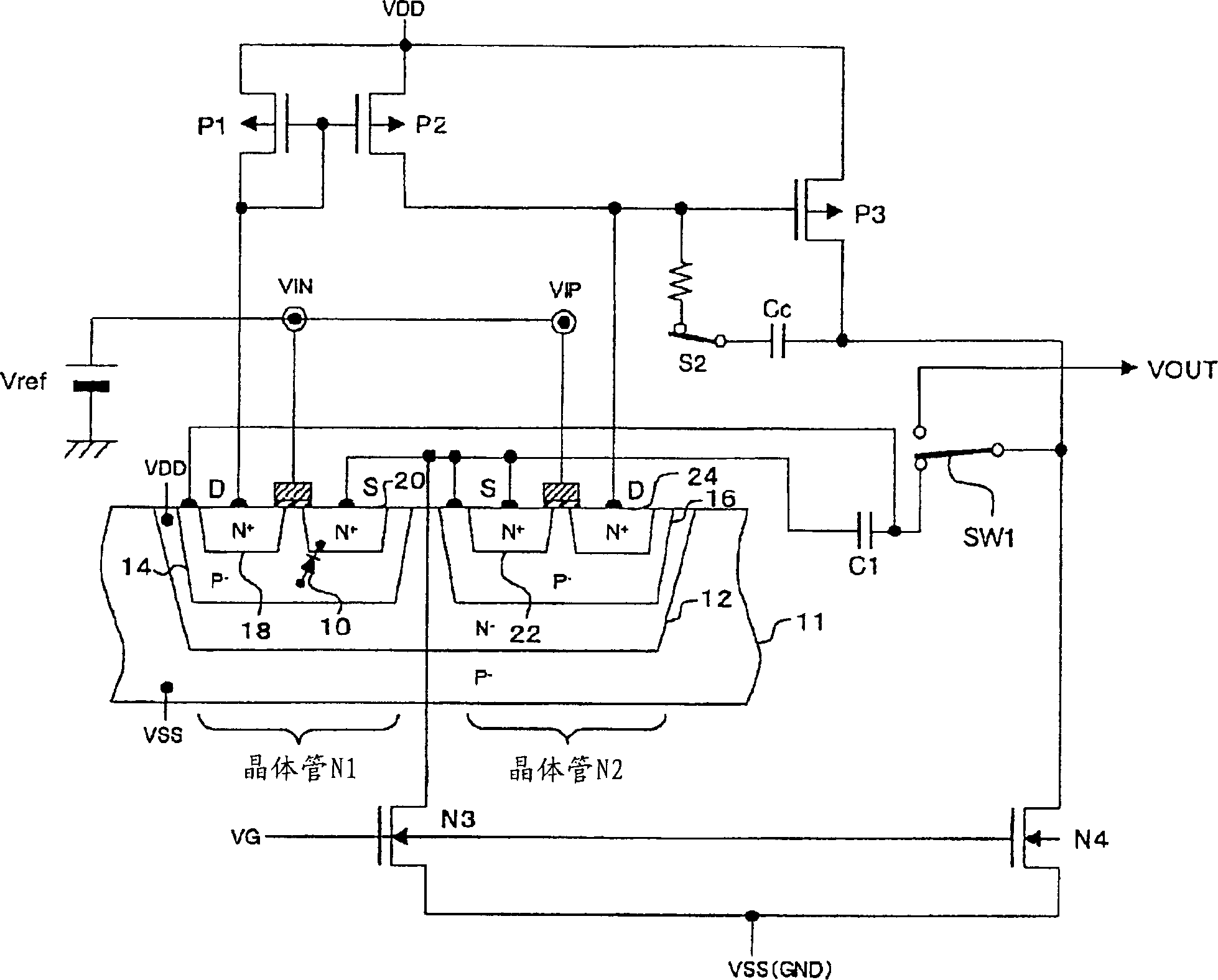
[0059] figure 1 is a circuit diagram showing the structure of the comparison circuit according to the first embodiment of the present invention. As shown in the figure, the comparison circuit (hereinafter also referred to as "comparator") is configured with: NMOS transistors M1 and M2 for forming a differential pair; constant current source transistor N3; load transistors (PMOS transistors) P1 and P2, Used to form a current mirror; and an output stage transistor (composed of a PMOS transistor P3 and a constant current source transistor N4), used to form a push-pull output stage circuit. This comparison circuit is also configured with: a phase adjustment resistor Rc; a phase adjustment capacitor Cc; a phase adjustment circuit 410 composed of a switch SW2 which becomes ON when bias is adjusted; a DC cut capacitor C1; a switch SW1; a switch SW2; another switch SW3; an input T1; and another input T2.

[0060] In this case, an input voltage (INPUT) or a reference voltage (also re...

no. 2 example

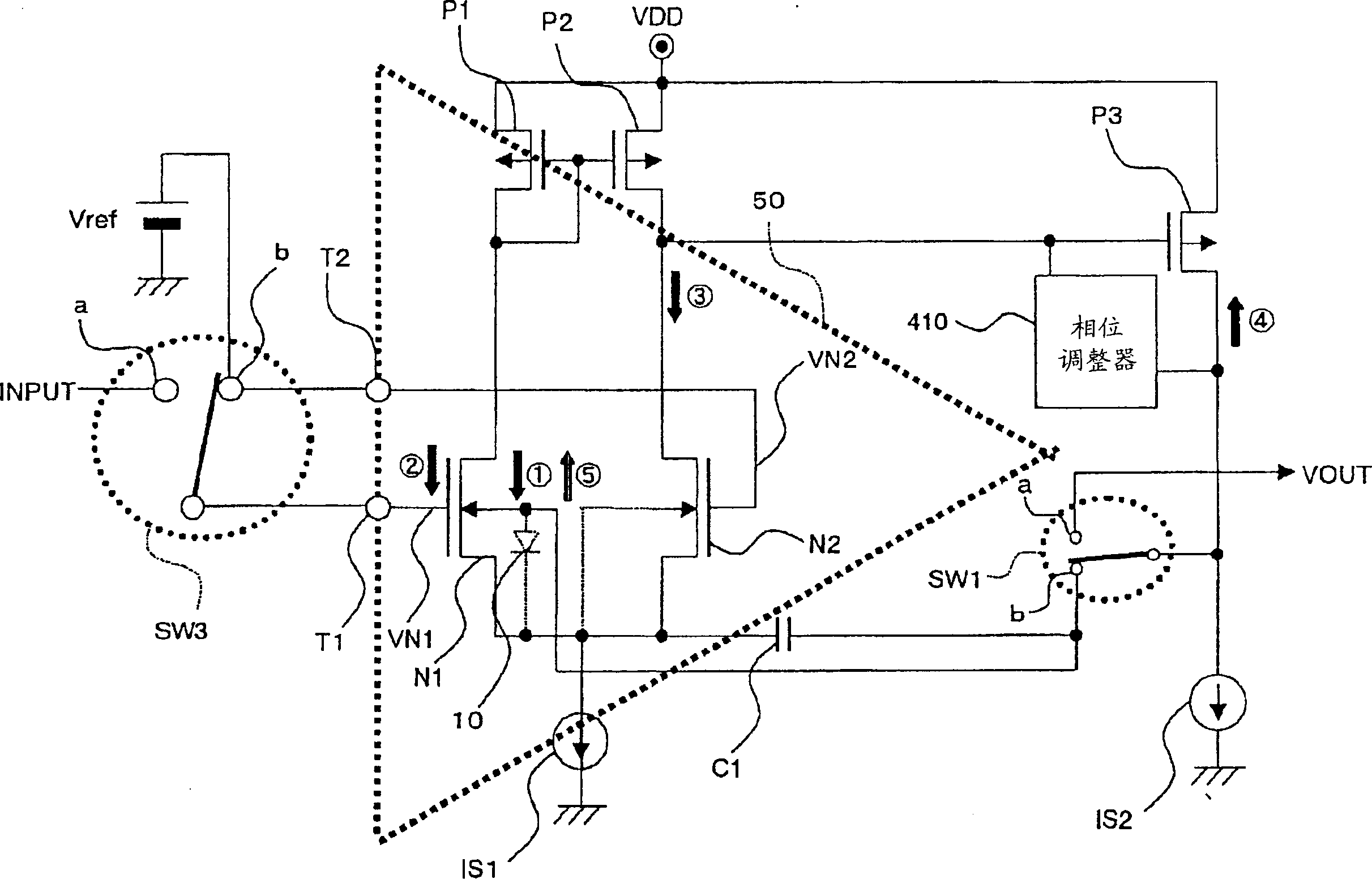
[0116] Figure 10 A structural circuit diagram of the bias compensation device according to the second embodiment mode of the present invention is shown. The offset compensating device of this second embodiment can cancel a DC offset by using a comparator having an offset adjustment function.

[0117] In this second embodiment, for the comparator, the comparator 400 equipped with the offset adjustment function as described in the first embodiment is used. Before canceling the bias of the D / A converter 500a (500b), the switch SW4 provided at the input stage of the comparator 400 is switched to the "a" side terminal in order to adjust the right / left current bias. The differential output (negative) of the D / A converter 500a (500b) is input to the "a" terminal.

[0118]As a result, the comparison voltage used in the comparator 400 is equivalent to the difference between the reference voltage "Vref" connected to the non-inverting terminal of the comparator 400 and the D / A convert...

no. 3 example

[0128] Figure 11 A structural circuit diagram of a bias compensation device according to a third embodiment mode of the present invention is shown. It should be understood that the same reference numerals shown in the second embodiment are used to denote the same or similar circuit elements used in the third embodiment. In the offset compensation device of the third embodiment, the correction value generation circuit 430 is composed of an addition and subtraction circuit (up / down counter) 432 and a latch 434, and the value from the addition and subtraction circuit 432 can be selected by the switch SW5. Any one of the output signals is used as an input signal to the adder 420 . Other circuit configurations of this bias compensation device are similar to Figure 10 The structure of the circuit shown.

[0129] In this embodiment, for the comparator, the comparator 400 equipped with the offset adjustment function as explained in the above-mentioned first embodiment is used. B...


PUM


Abstract

Comparator circuit and bias compensator. While a switch SW4 is connected to 'a'-terminal side, offset of a differential output voltage 'A-' of a D / A converter 500a (500b) is held in a comparator 400, and is reflected to a reference voltage. Thereafter, the switch SW4 is switched to a 'b'-terminal side, and offset of a differential output voltage 'A+' of the D / A converter 500a (500b) is measured by the comparator 400. An error signal is outputted to a counter 412 so as to count up the counter 412. Such an operation is repeatedly carried out in which the count value is added to 1.7 V and then the added count value is inputted into the D / A converter 500a (500b), and such a count value latched in a latch at timing when the error signal is inverted is defined as an offset correction value.

Description

technical field [0001] The present invention relates to an offset compensating device for compensating a DC offset voltage of a D / A converter such as used in a digital radiotelephone, and also relates to a device used in the offset compensating device for measuring D Comparator circuit for the bias of the / C converter. Background technique [0002] In digital radiotelephones, the signal to be transmitted is modulated in the digital circuit portion of the modulator. Afterwards, the modulated digital signal is converted into an analog signal by a D / A converter. The converted analog signal is coupled to the radio frequency unit of the digital radiotelephone for transmission as a radio signal. Such a D / A converter causes the following problems. [0003] That is, there are some cases where a DC offset having a low level is generated in the analog output of the D / A converter, and the DC offset changes slowly. Usually, the occurrence of this DC offset is caused by the fact that...

Claims


Application Information

Patent Timeline
Patent Type & Authority Applications(China)
IPC IPC(8): H03F3/45H03K5/08H03M1/10H03M1/66
CPCH03F3/45H03M1/1019H03M1/66
Inventor 森宏一多田有作
Owner PANASONIC CORP
Why Eureka
Try Eureka