Copper foil with carrier foil, process for producing the same and copper clad laminate including the copper foil with carrier foil
A manufacturing method and carrier foil technology, applied in the field of copper foil, can solve the problems of rising production costs, insolubility, and increased operating costs of printed circuit boards
- Summary
- Abstract
- Description
- Claims
- Application Information
AI Technical Summary
Problems solved by technology
Method used
Image
Examples
Embodiment 1
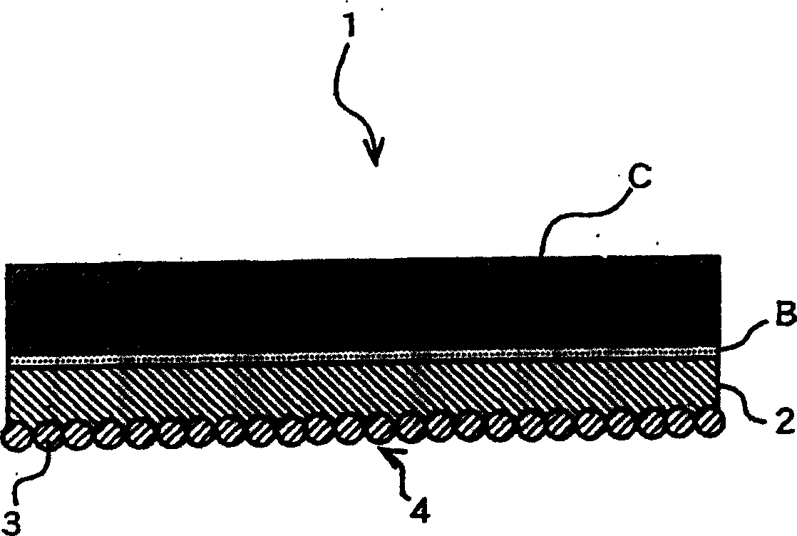
[0068] In this example, according to Figure 6 The sequence shown produces a copper foil with carrier foil 1 whose main copper layer 2 consists entirely of high-carbon copper. exist Figure 6 In the process shown in (a), first, 18 μm thick copper foil is used as the carrier foil C, and the surface of the carrier foil C is pickled to completely remove the adhering grease components, and then remove the residual surface oxide film. For the pickling treatment, a dilute sulfuric acid solution with a concentration of 100 g / l and a liquid temperature of 30° C. was used, and the immersion time was 30 seconds.
[0069] The carrier foil C that has finished the pickling treatment is immersed in an aqueous solution containing CBTA at a concentration of 5g / l, a liquid temperature of 40°C, and a pH of 5 for 30 seconds. Figure 6 As shown in (b), a bonding interface layer is formed on the surface. Strictly speaking, when this dipping method is used, the joint interface layer B is formed ...
Embodiment 2
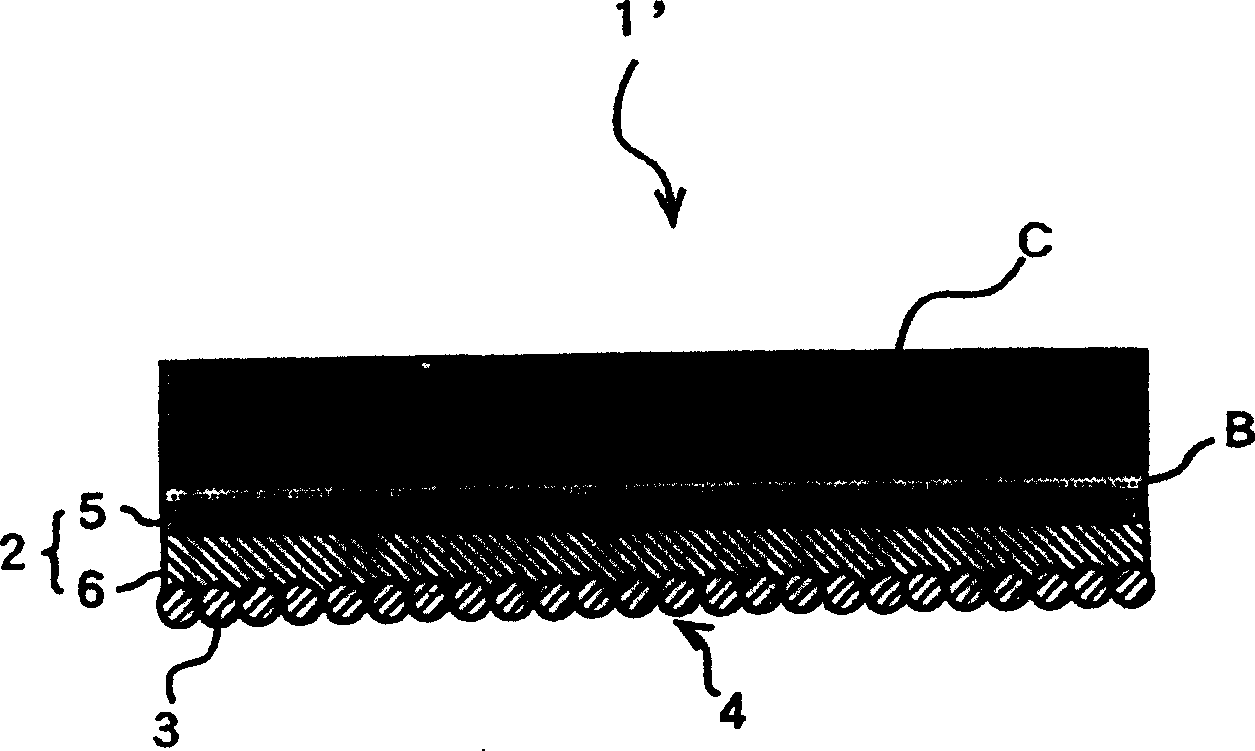
[0078] In this example, according to Figure 8 The shown procedure produces a copper foil with carrier foil 1' in which the main copper layer 2 is composed of a high-carbon copper layer 5 with a thickness of 3 µm and a pure copper layer 6 with a thickness of 3 µm. The carrier foil C used here was the same copper foil with a thickness of 18 μm as in Example 1, and the pickling treatment on the surface of the carrier foil C and the formation of the bonding interface layer B after the pickling treatment were also the same as in Example 1. The roughening treatment and antirust treatment after the formation of the main body copper layer 2 are the same as those in Example 1, so the description will not be repeated. These descriptions are omitted here, and only the formation of the main body copper layer 2 will be described in detail.
[0079] After the joint interface layer B was formed, the carrier foil C on which the joint interface layer B was formed was subjected to cathodic po...
PUM
| Property | Measurement | Unit |
|---|---|---|
| thickness | aaaaa | aaaaa |
| thermal conductivity | aaaaa | aaaaa |
| thermal conductivity | aaaaa | aaaaa |
Abstract
Description
Claims
Application Information


