

Producing method for thin-membrane transistor liquid-crystal displaying device
A liquid crystal display and thin film transistor technology, applied in semiconductor/solid-state device manufacturing, instruments, optics, etc., can solve the problems of complex etching process, cross-cut, affecting TFT-LCD display, etc., to ensure the quality of the effect.
- Summary
- Abstract
- Description
- Claims
- Application Information
AI Technical Summary
Problems solved by technology
Method used
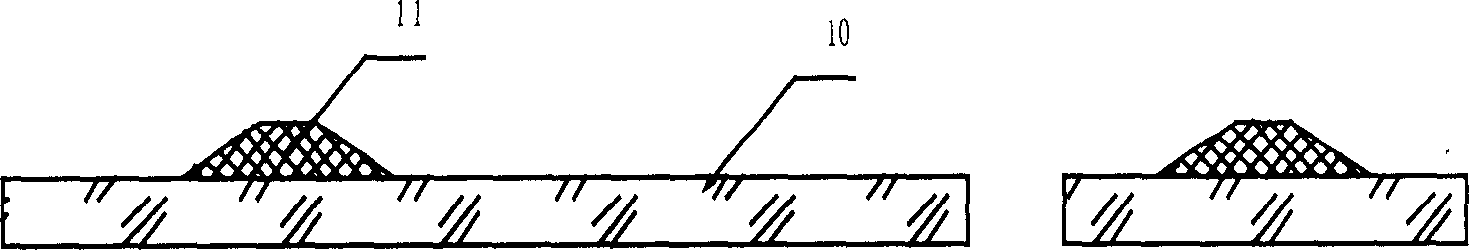
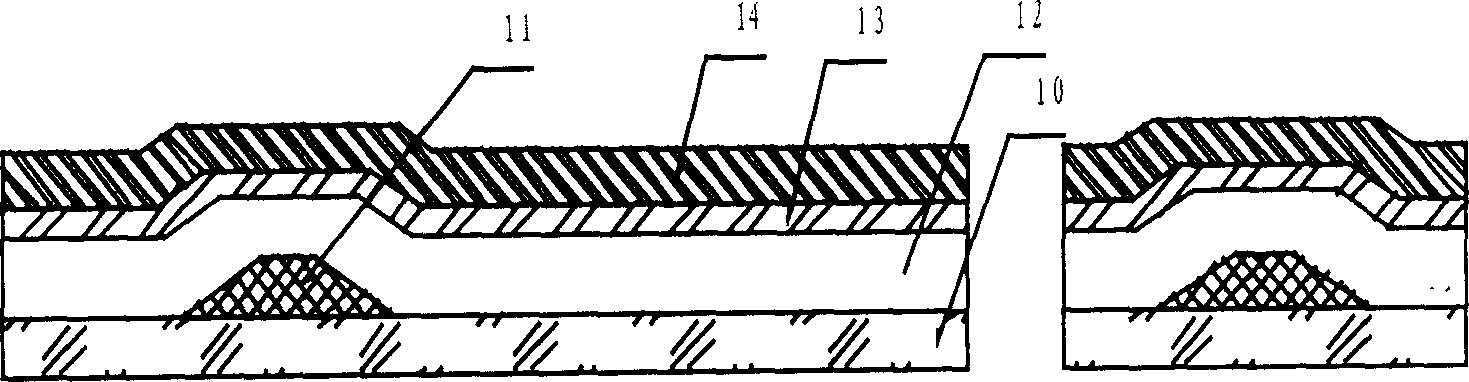
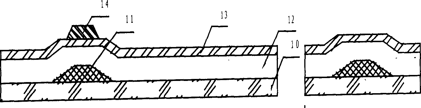
Image

Examples
Embodiment Construction
[0032] In order to understand the purpose, features and advantages of the present invention more clearly, the present invention will be further described below in conjunction with the accompanying drawings and embodiments.
[0033] Please refer to FIG. 2a-FIG. 2h, which are schematic cross-sectional steps of a preferred embodiment of the TFT-LCD manufacturing method developed by the present invention to improve the prior art.
[0034] As shown in FIG. 2 a : firstly, a first metal layer is deposited on the surface of the glass substrate 30 (it can be done by molybdenum-tungsten alloy, chromium, aluminum, aluminum alloy or copper). Then, the first photolithography process is performed to etch the first metal layer to form the gate electrode 31 and the scanning lines (not shown) connected to the gate electrode 31 .
[0035] As shown in FIG. 2b: after the first photolithography and etching process is completed, a gate insulating layer 1 32a and a gate insulating layer 2 32b are se...
PUM
 Abstract
Description
Claims
Application Information