

Silicon photoelectric probe compatible with deep submicron radio frequency technology
A deep submicron, silicon photoelectric technology, applied in photometry, electrical solid-state devices, optical radiation measurement, etc., can solve problems such as limiting the range of optical fiber coupling activities, large parasitic capacitance, etc., to achieve high yield, improve performance, and high speed effect
- Summary
- Abstract
- Description
- Claims
- Application Information
AI Technical Summary
Problems solved by technology
Method used
Image

Examples
Embodiment Construction
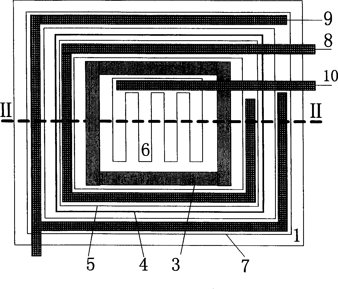
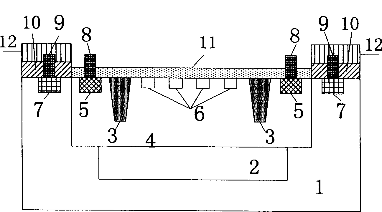
[0015] The present invention is achieved by the following methods: figure 1 Shows the layout structure of the photodetector for fabrication on deep submicron RF_CMOS process, figure 2 A longitudinal cross-sectional structure diagram of the photodetector is shown, mainly showing the longitudinal dimension of the photodetector.
[0016] P-type semiconductor substrate 1, deep n-type well 2, the deep n-type well 2 is fabricated in the substrate 1; n-type well 4, the n-type well 4 is fabricated on the substrate 1; shallow trench isolation region 3 , the shallow trench isolation region 3 is fabricated in the n-type well 4; four interdigitated P+ type diffusion regions 4, the four interdigitated P+ + Type diffusion region 6 is set on n-type well 4; P + Type guard ring 7, the P + type guard ring 7 is fabricated on the substrate 1 and around the n-type well 4; the anti-reflection coating layer 11 is deposited on four interdigitated P + Type diffusion region 6 above; by the interdi...
PUM
 Abstract
Description
Claims
Application Information