Design method of 0.35 um LDMOS high vltage power displaying driving element
A design method and display driving technology, applied in the direction of electric solid-state devices, semiconductor devices, static indicators, etc., can solve the problems of large total area of die, large working current, difficulty in shortening channel length, etc.
- Summary
- Abstract
- Description
- Claims
- Application Information
AI Technical Summary
Problems solved by technology
Method used
Image

Examples
Embodiment
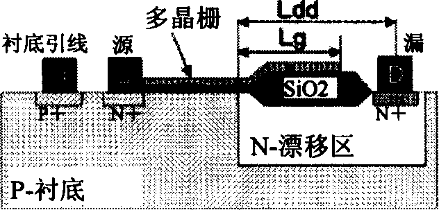
[0061] Figure 5 is the actual layout of the driving device composed of 4 0.35μm, LD-NMOS units connected in parallel (for clarity, some details are gated out). The channel length of the unit device is L=0.35μm, the total width W=160μm, and the gate oxide layer d ox =100,open voltage V T =0.7V. At gate voltage V G =4V, leakage current I D = 1mA / μm. 160 rows of drive array, unit area 28×40=1120μm 2 , The total area is 160×28×40=4480×40μm 2 . It can be changed to 160×14×80=2240×80μm according to needs 2 arrangement. In the latter arrangement, the wire current density reaches 1.6×10 6 / cm 2 , But because the duty cycle is less than 0.01, this scheme is feasible.
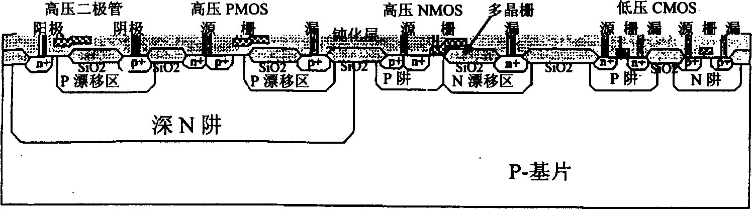
[0062] The plan view and the cross-sectional structure of LDPMOS are similar, but the doping is different. The most important difference is that the total channel width of the P tube is about 20 μm, which is 1 / 8 of the N tube, because it does not need to bear too much current.
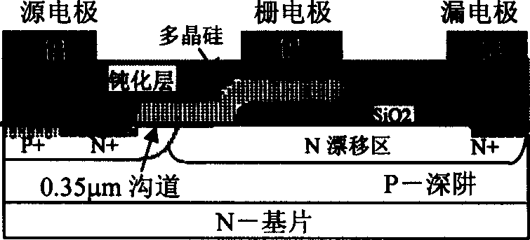
[0063] Figure 6 is The layout of the lead c...
PUM
 Abstract
Description
Claims
Application Information
 - R&D Engineer
- R&D Manager
- IP Professional
- Industry Leading Data Capabilities
- Powerful AI technology
- Patent DNA Extraction
Browse by: Latest US Patents, China's latest patents, Technical Efficacy Thesaurus, Application Domain, Technology Topic.
© 2024 PatSnap. All rights reserved.Legal|Privacy policy|Modern Slavery Act Transparency Statement|Sitemap