
Eureka
For R&D, Eureka makes reading and utilizing patents & technical documents easy.
Eureka AIR
Designed for self-driven R&D workflows. Generate viable solutions, solve complex R&D challenges, empower your innovation with AI.

Eureka Materials
Designed for material experts only. Revolutionize your material R&D, from search, analyze, to developing new materials.

TechResearch
Generate reliable direction feasibility study reports for your R&D in just a few steps.

TechSeek
Discover and master advanced knowledge NOW. Basics, ideas, possibilities, all at once.

TechMind
As an expert in R&D Theories, TechMind can generates customized viable solutions instantly.

TechRisk
Analyze your overall solution with one click, know your potential R&D risks in advance.

TechMonitor
Get weekly tech updates, stay abreast of the latest tech innovations and key insights.
Method for preparing indium-gallium-arsenic material of gradation band gap
A technology of indium gallium arsenide and indium phosphide is applied in the field of preparation of materials for active regions of semiconductor optoelectronic devices, and can solve the problems of complex production degree and the like
- Summary
- Abstract
- Description
- Claims
- Application Information
AI Technical Summary
Problems solved by technology
Method used
Image

Examples
preparation example Construction
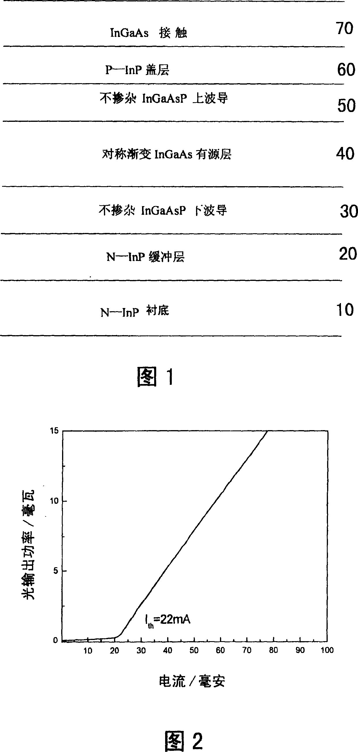
[0027] Please refer to FIG. 1, a method for epitaxy preparation of a graded InGaAs material according to the present invention is characterized in that it includes the following steps:
[0028] (1) epitaxially grow one layer of indium phosphide or gallium arsenide buffer layer 60 on substrate 70, said substrate 70 is indium phosphide substrate or gallium arsenide substrate; said buffer layer 60 is phosphorus An indium buffer layer, the thickness of the buffer layer is about 1 μm;
[0029] (2) epitaxially growing a lower waveguide layer 50 on the buffer layer 60;
[0030] (3) epitaxially growing the graded InGaAs active layer 40 on the lower waveguide layer 50 , when growing the graded InGaAs material, the growth temperature is between 600° C. and 630° C., and the growth pressure is 50 mbar;
[0031] (4) Next, grow an undoped waveguide layer 30 on the graded InGaAs active layer 40;
[0032] (5) The upper waveguide cover layer 20 is grown on the undoped waveguide layer 30, whe...
Embodiment
[0036] The invention is a quasi-continuously strained InGaAs (indium gallium arsenic) bulk material grown by LP-MOVPE (low pressure-metal organic vapor phase epitaxy), and obtains the desired Strain, the technical solution is as follows (taking InP (indium phosphorus) base as an example) (see Figure 1 in combination):
[0037] 1) The cleaned InP substrate is placed in a MOVPE (metal organic vapor phase epitaxy) reaction chamber (not shown in the figure);
[0038] 2) Epitaxial growth of a lower waveguide layer matching the InP lattice on the InP substrate 70 (the pressure in the reaction chamber is 22 mbar, and the temperature is 650 degrees Celsius);
[0039] 3) Epitaxial growth of graded InGaAs bulk material on the lower waveguide layer. When growing this layer of graded InGaAs bulk material, the key is to control the source flow of TMGa during the growth process, so that the source flow of TMGa has a large mismatch with the substrate InP The amount (this amount corresponds ...
PUM
 Abstract
Description
Claims
Application Information
 - R&D Engineer
- R&D Manager
- IP Professional
- Industry Leading Data Capabilities
- Powerful AI technology
- Patent DNA Extraction
Browse by: Latest US Patents, China's latest patents, Technical Efficacy Thesaurus, Application Domain, Technology Topic, Popular Technical Reports.
© 2024 PatSnap. All rights reserved.Legal|Privacy policy|Modern Slavery Act Transparency Statement|Sitemap|About US| Contact US: help@patsnap.com