Booster circuit, semiconductor device, and display device

A booster circuit and semiconductor technology, which is applied in the field of semiconductor devices, display devices, and booster circuits, can solve problems such as increased current consumption, and achieve the effects of reducing charge and discharge currents, reducing costs, and reducing manufacturing costs

Inactive Publication Date: 2005-02-02
SEIKO EPSON CORP
View PDF0 Cites 2 Cited by
  • Summary
  • Abstract
  • Description
  • Claims
  • Application Information

AI Technical Summary

Problems solved by technology

Therefore, in order to obtain the same performance as the conventional boost circuit with an external capacitor, it is necessary to increase the switching frequency of the switching element in the charge pump circuit, resulting in an increase in current consumption due to an increase in the charge and discharge current of the capacitor.

Method used


Image

  • Booster circuit, semiconductor device, and display device
  • Booster circuit, semiconductor device, and display device
  • Booster circuit, semiconductor device, and display device

Examples


Embodiment Construction

[0066] Hereinafter, preferred embodiments of the present invention will be described in detail with reference to the accompanying drawings. In addition, the embodiment described below does not unduly limit the content of the present invention described in the claims. Furthermore, not all components described below are necessarily essential components of the present invention.

[0067] 1. Outline of the booster circuit according to the present embodiment

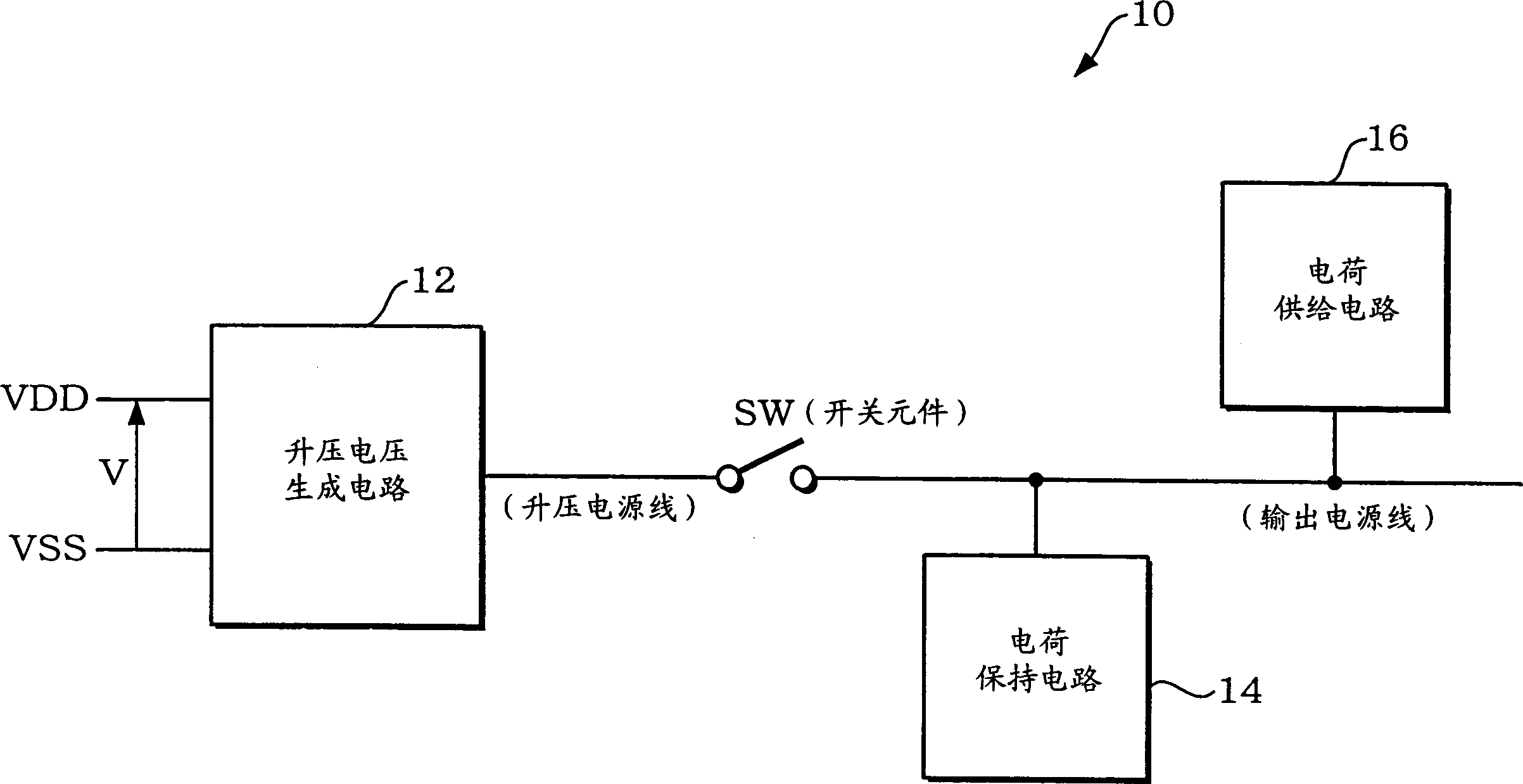
[0068] exist figure 1 In , the composition diagram of the boost circuit according to this embodiment is given. The boost circuit 10 outputs a boosted voltage obtained by boosting a voltage V between a system power supply voltage VDD and a ground power supply voltage VSS to an output power supply line. The output power line is connected to a device (load) using the boosted voltage.

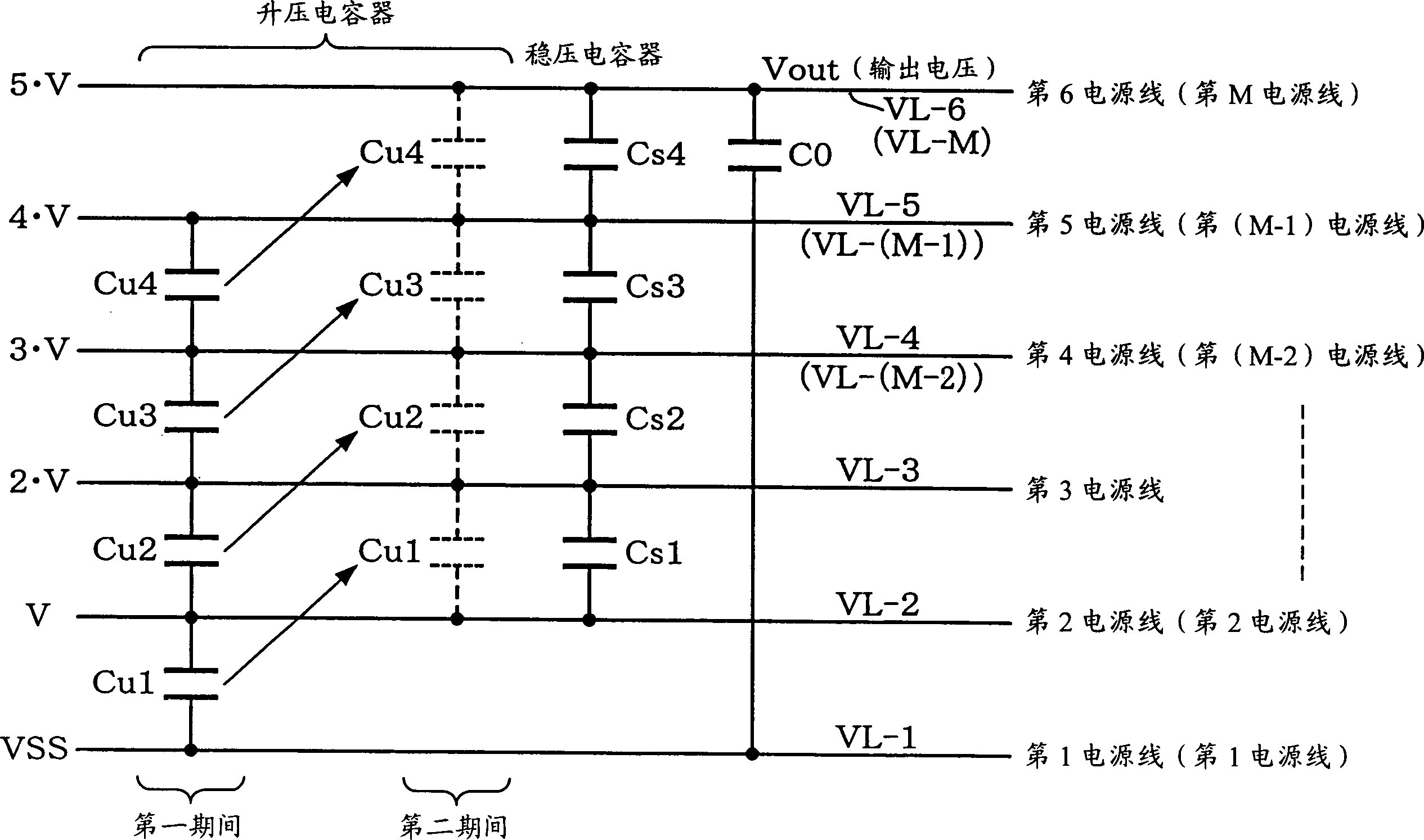
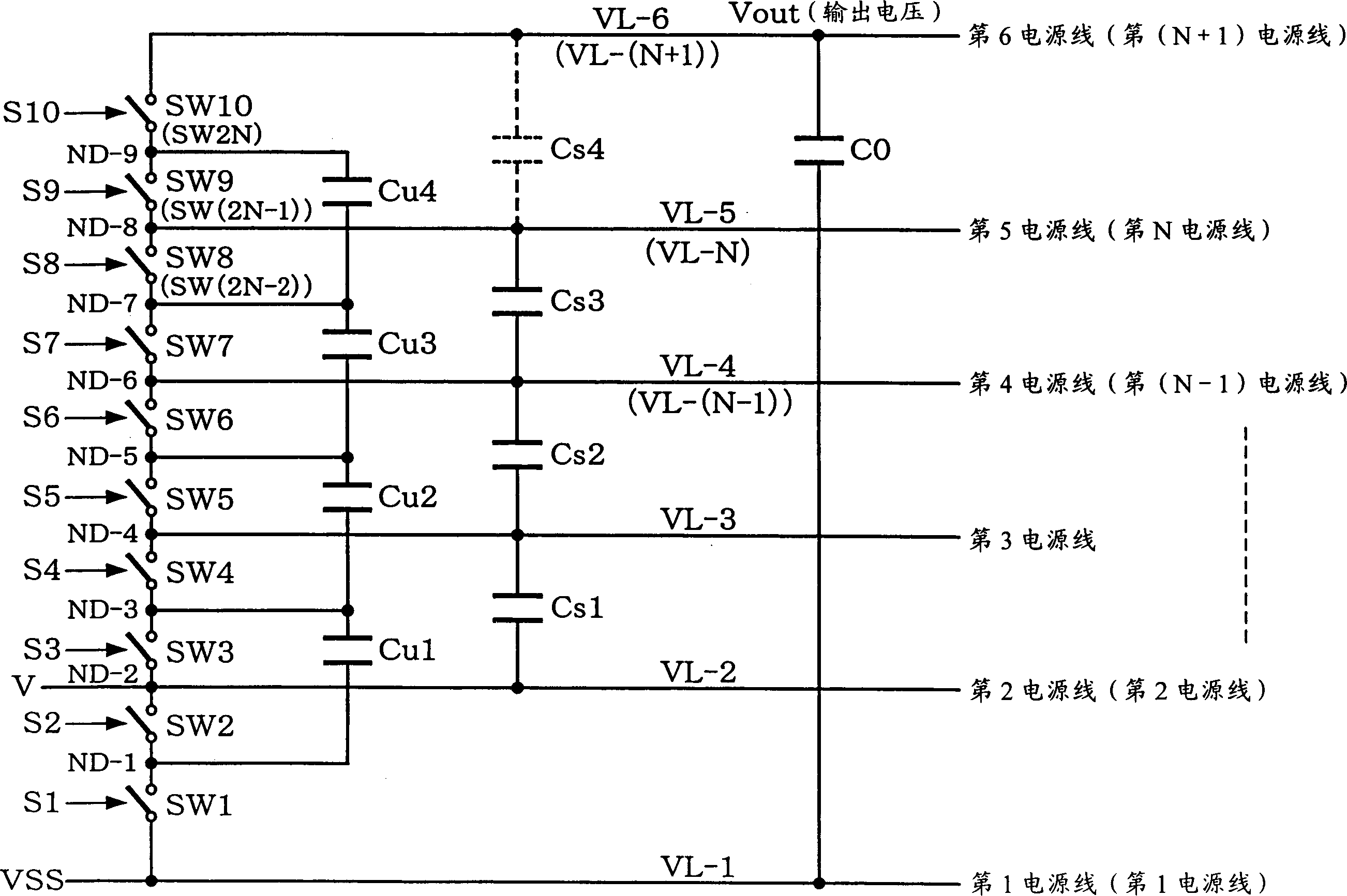
[0069] The boost circuit 10 includes a boost voltage generating circuit 12 , a switching element SW, a charge holding circuit 14 , and a char...


PUM


Abstract

A booster circuit including first to Mth power supply lines (VL-1 to VL-M) (M is an integer larger than 4) and first and second charge-pump circuits. Each of the charge-pump circuit has first to (M-2)th boost capacitors (Cu1 to Cu(M-2)), wherein the jth boost capacitor (1<=j<=M-2, j is an integer) is connected between the jth power supply line and the (j+1)th power supply line in a first period and is connected between the (j+1)th power supply line and the (j+2)th power supply line in a second period subsequent to the first period. Each of the charge-pump circuits generates a boosted voltage by a charge-pump operation in different phases.

Description

technical field [0001] The invention relates to a boost circuit, a semiconductor device and a display device. Background technique [0002] As the display device, a liquid crystal display device including an electro-optical device can be used. Mounting a liquid crystal display device in an electronic device can simultaneously achieve miniaturization and low power consumption of the electronic device. [0003] However, driving a liquid crystal display device requires a high voltage. Therefore, it is also suitable in terms of cost to incorporate a power supply circuit for generating a high voltage in a driver IC (Integrated Circuit) (semiconductor device in a broad sense) that drives an electro-optical device. At this time, the power supply circuit includes a boost circuit. The boost circuit boosts the voltage between the system power supply voltage VDD on the high potential side and the ground power supply voltage VSS on the low potential side to generate an output voltage...

Claims


Application Information

Patent Timeline
Patent Type & Authority Applications(China)
IPC IPC(8): H01L27/04H01L21/822H02M3/07
CPCH02M3/07H02M2001/009H02M1/009
Inventor 上条治雄
Owner SEIKO EPSON CORP
Why Eureka
Try Eureka