Method for remaking etching suspension layer

An etching method and etching technology, applied in optics, instruments, electrical components, etc., can solve the problems of incomplete amorphous silicon channel layer, great influence on TFT process and finished product qualification rate, over-etching of the second silicon nitride layer 110, etc.

Inactive Publication Date: 2005-02-16
AU OPTRONICS CORP
View PDF0 Cites 1 Cited by
  • Summary
  • Abstract
  • Description
  • Claims
  • Application Information

AI Technical Summary

Problems solved by technology

[0011] It should be noted that, in the process of etching the second silicon nitride layer 110 in FIG. The semiconductor structure 140 composed of the silicon oxide layer 106, the first silicon nitride layer 107, the amorphous silicon layer 108, the second silicon nitride layer 110, and the patterned photoresist layer 111 stays in the etching tool for too long. For a long time, the overetching phenomenon of the second silicon nitride layer 110 occurs
For example, when the semiconductor structure 140 stays in the etching machine for a long time, part of the etch stop layer is damaged due to the corrosion of residual acid, and the patterned photoresist layer 111 may be peeled off, because the formed The etch stop layer is defective and cannot meet the standard specification requirements
Then, in the process of forming the N+ ohmic contact layer, the incomplete etching stop layer will not be able to protect the part of the amorphous silicon channel layer below it from being removed during the etching process, so that the formed amorphous silicon channel layer also produces incomplete Phenomenon, which has a great influence on the electrical quality
Therefore, the semiconductor structure with the incomplete etch stop layer and the substrate cannot continue to be used and must be scrapped and discarded, which has a great impact on the TFT process and the yield of finished products

Method used


Image

  • Method for remaking etching suspension layer
  • Method for remaking etching suspension layer
  • Method for remaking etching suspension layer

Examples


Embodiment Construction

[0033] In order to make the above-mentioned purposes, features and advantages of the present invention more obvious and understandable, a preferred embodiment is specifically cited below, together with the accompanying drawings, and the detailed description is as follows:

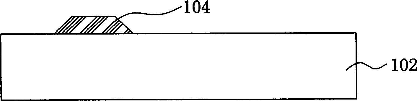
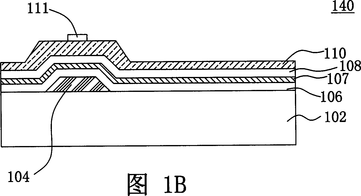
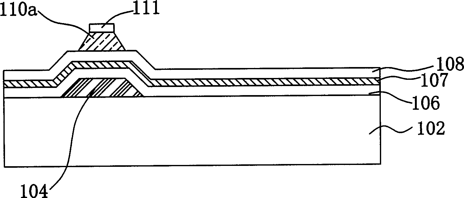
[0034] The present invention provides a method for reworking an etching-stop layer, which is used on a semiconductor structure. The semiconductor structure includes a substrate, a gate, a gate insulating layer, and an amorphous silicon (amorphous silicon, α-Si) layer, an incomplete etch stop layer and a first patterned photoresist layer. Wherein, the gate is formed on the substrate, the gate insulating layer is formed on the substrate, and the gate insulating layer covers the gate. The amorphous silicon layer is formed on the grid insulating layer, the incomplete etch stop layer is formed on the amorphous silicon layer, and the first patterned photoresist layer is formed on the incomplete etch stop layer. ...


PUM


Abstract

In the invention, semiconductor structure includes an amorphous silicon layer, an incomplete etching stopped layer, and first patterned photoresist layer. The incomplete etching stopped layer is formed on the amorphous silicon layer. The first patterned photoresist layer is formed on the incomplete etching stopped layer. The procedure for remaking etching stopped layer includes following steps: removing first patterned photoresist layer, incomplete etching stopped layer; cleansing surface of the amorphous silicon layer by using N+ precleaning method; processing serface of the amorphous silicon layer through hydrogen gas-plasma, and forming a silicon nitride layer on the amorphous silicon layer by using method of chemical vapor deposition; forming second patterned photoresist layer on the said silicon nitride layer, and removing exposed partial silicon nitride layer through etching.

Description

technical field [0001] The present invention relates to a kind of thin film transistor (thin film transistor, TFT) manufacturing method, and particularly relate to a kind of incomplete etch stop layer (etching-stoplayer) that can remove on the amorphous silicon layer (etching-stoplayer) and form a rework on the amorphous silicon layer method of etching stop layer. Background technique [0002] Liquid crystal displays (LCDs) are widely used due to their advantages of low radiation and small size. TFT LCD is very popular in high-end electronic products because of its high brightness and large viewing angle. [0003] A traditional TFT LCD is composed of a TFT panel and a color filter (color filter, CF) panel. The color filter CF panel includes at least a common electrode (common electrode) and RGB color filters, and the TFT panel has It includes a substrate, a plurality of scan lines, a plurality of data lines, a plurality of storage capacitors, a plurality of TFTs and a plur...

Claims


Application Information

Patent Timeline
Patent Type & Authority Applications(China)
IPC IPC(8): G02F1/136H01L21/00
Inventor 徐书扬洪汝豪张世国张全光
Owner AU OPTRONICS CORP
Why Eureka
Try Eureka