Intermittent feeding technique for increasing the melting rate of polycrystalline silicon

A polysilicon, intermittent technology, applied in the direction of polycrystalline material growth, single crystal growth, single crystal growth, etc., can solve problems such as slow feeding rate

Inactive Publication Date: 2005-02-23
MEMC ELECTONIC MATERIALS INC
View PDF4 Cites 5 Cited by
  • Summary
  • Abstract
  • Description
  • Claims
  • Application Information

AI Technical Summary

Problems solved by technology

Much of this slower feed rate is due to the aforementioned limitations of the crucible

Method used


Image

  • Intermittent feeding technique for increasing the melting rate of polycrystalline silicon
  • Intermittent feeding technique for increasing the melting rate of polycrystalline silicon
  • Intermittent feeding technique for increasing the melting rate of polycrystalline silicon

Examples


example 1

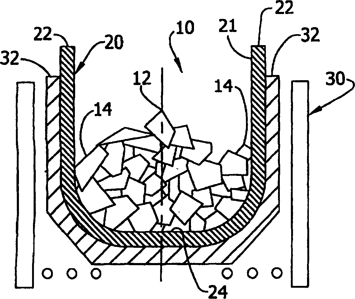
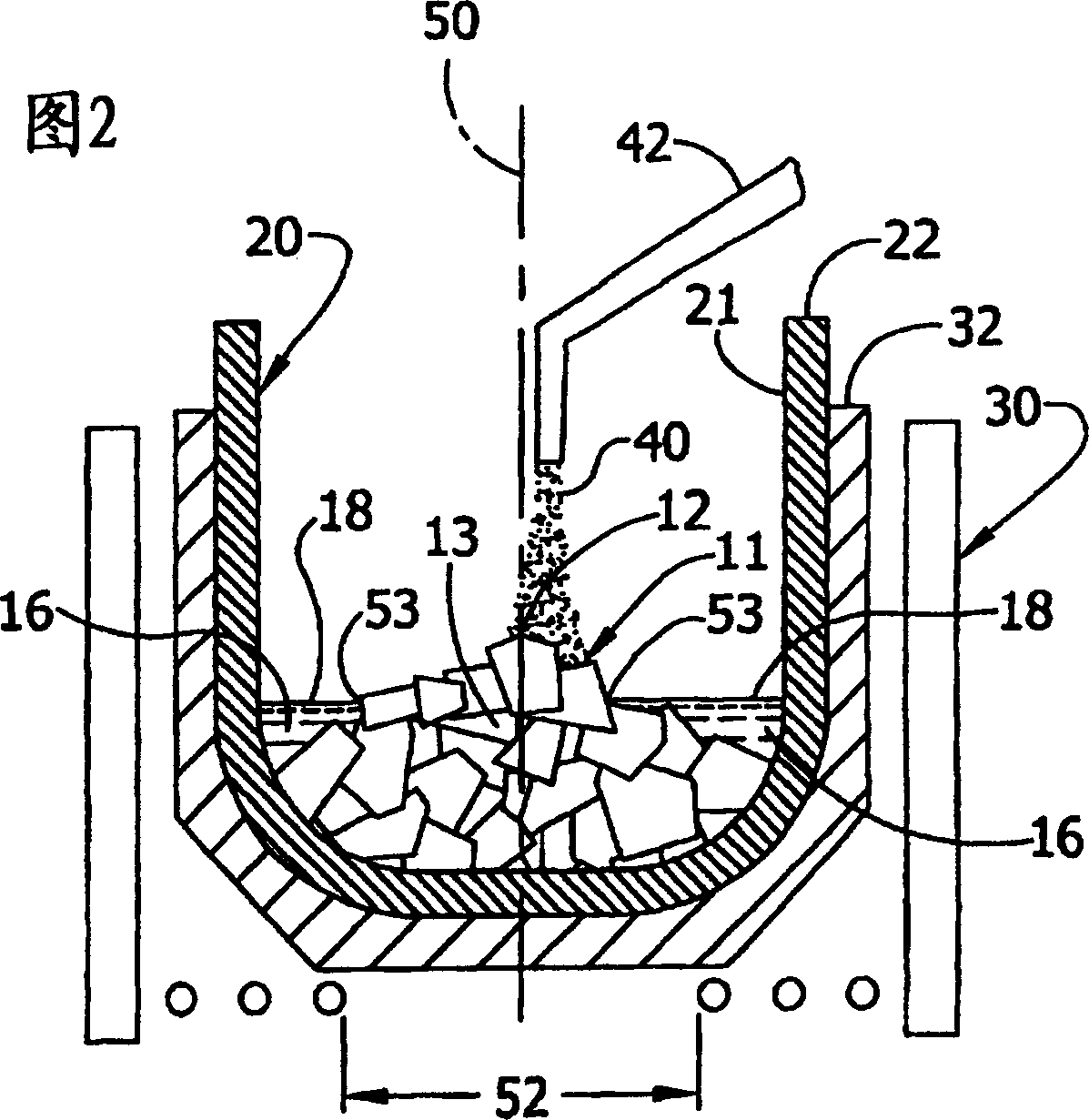
[0060] Approximately 40 kg of chunk polycrystalline silicon was charged into a 20 inch (51 cm) diameter crucible and heated to form molten silicon and unmelted polycrystalline silicon. Using a vertical feed tube positioned slightly off the centerline of the crucible (about 15 mm) and about 10 inches (25 cm) above the melt surface, about 40 kg of granular polysilicon was added to the crucible for a total charge of about 80 kg. The granular polysilicon flow rate (f) was about 17 g / sec from the hopper through the injector tube and into the crucible.

[0061] The furnace side heater power was about 118 kW, and the crucible rotation speed (r) was about 2 RPM (revolutions per minute). The bulk polysilicon was partially melted after about 3.5 hours (ie, the diameter of the islet of polysilicon centered in the crucible was about 75% of the crucible diameter). Initially, the duration of the duty cycle (t on ) is set to about 5 seconds and the duration of the rest period (t off ) was...

example 2

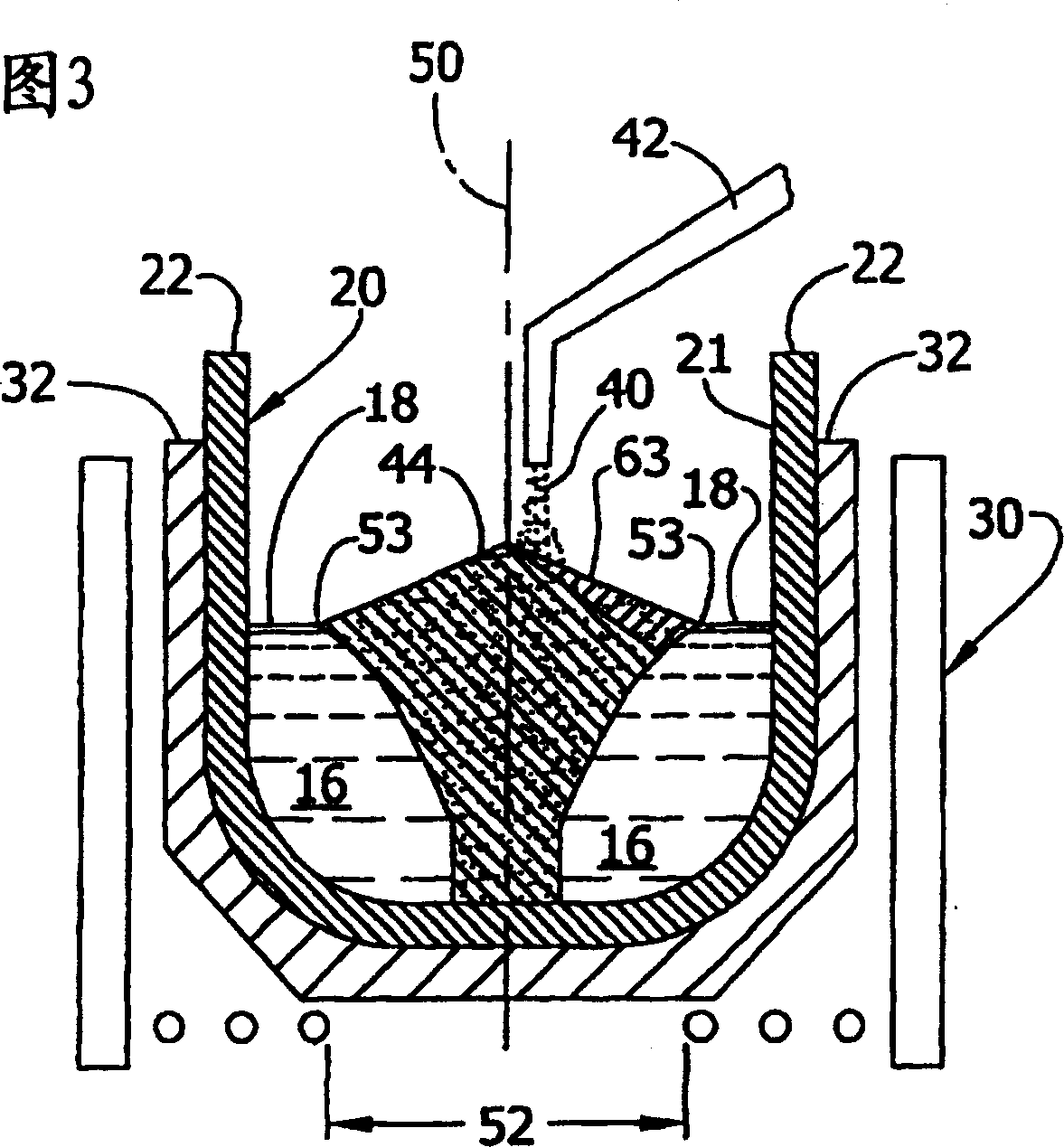
[0065] Based on the tests detailed in Example 1, it was determined that the batch feed method can greatly increase the feed rate (F) at which the proper island width can be maintained, thereby reducing the Feeding time. Specifically, it can be determined that maximizing the degree of rotation between successive (successive) stacked wedges and the number of duty cycles before the feed material is re-(re)stacked on a particular portion or segment of the polysilicon islet is maximized, greatly Increased the flow rate at which islet size can be maintained at 75% of the crucible diameter.

[0066] In view of the above principles, an optimum set of parameters was determined and tested to maximize the feed / melt rate of granular polysilicon in the loaded crucible. As in Example 1, the crucible was initially loaded with 40 kg chunk polycrystalline silicon, the gravity feeder delivered granular polycrystalline silicon at a flow rate (f) of about 17 g / s, and the side heater power was ab...


PUM

PropertyMeasurementUnit
angleaaaaaaaaaa

Abstract

A process for preparing a silicon melt in a crucible for use in growing a single crystal silicon ingot by the Czochralski method. The crucible is first loaded with chunk polycrystalline silicon and heated to partially melt the load. Granular polycrystalline silicon is then fed onto the exposed unmelted chunk polycrystalline silicon to complete the charge of silicon in the crucible. The granular polycrystalline silicon is intermittently delivered using a plurality of alternating on-periods and off-periods. During each on-period, granular polycrystalline silicon is flowed through a feed device that directs the granular polycrystalline silicon onto the unmelted chunk polycrystalline silicon. During each off-period, the flow of the granular polycrystalline silicon is interrupted. The loaded chunk polycrystalline silicon and the fed granular polycrystalline silicon are melted to form the silicon melt.

Description

technical field [0001] This invention relates generally to the production of single crystal silicon and, in particular, to a method for adding granular polycrystalline silicon to the preparation of silicon melts. Background technique [0002] Most of the single crystal silicon used in the manufacture of microelectronic circuits is prepared by the Czochralski method (CZ method). In this method, a monocrystalline silicon ingot is produced by melting polycrystalline silicon in a crucible; dipping a seed crystal into the silicon melt; pulling the seed crystal in a manner sufficient to achieve the desired diameter of the ingot; and Single crystals are grown at that diameter. The polysilicon that is melted to form the silicon melt is usually irregularly shaped bulk polysilicon produced by the Siemens process, or alternatively, free-flowing, generally spherical granular form, usually produced by the fluidized bed reaction process. polysilicon. Preparation and Properties of Bulk ...

Claims


Application Information

Patent Timeline
Patent Type & Authority Applications(China)
IPC IPC(8): C30B29/06C30B15/02
CPCC30B15/02
Inventor J·D·霍尔德
Owner MEMC ELECTONIC MATERIALS INC
Why Eureka
Try Eureka