

Composite material and chip holding component and making method thereof
A technology for composite materials and holding components, applied in chemical instruments and methods, semiconductor/solid-state device manufacturing, metal material coating technology, etc., can solve problems such as chip detachment, chip position shifting, chip damage, etc., to achieve residual adsorption The effect of small force, high reliability, and small strength fluctuation
- Summary
- Abstract
- Description
- Claims
- Application Information
AI Technical Summary
Problems solved by technology
Method used
Image

Examples
Embodiment approach 1
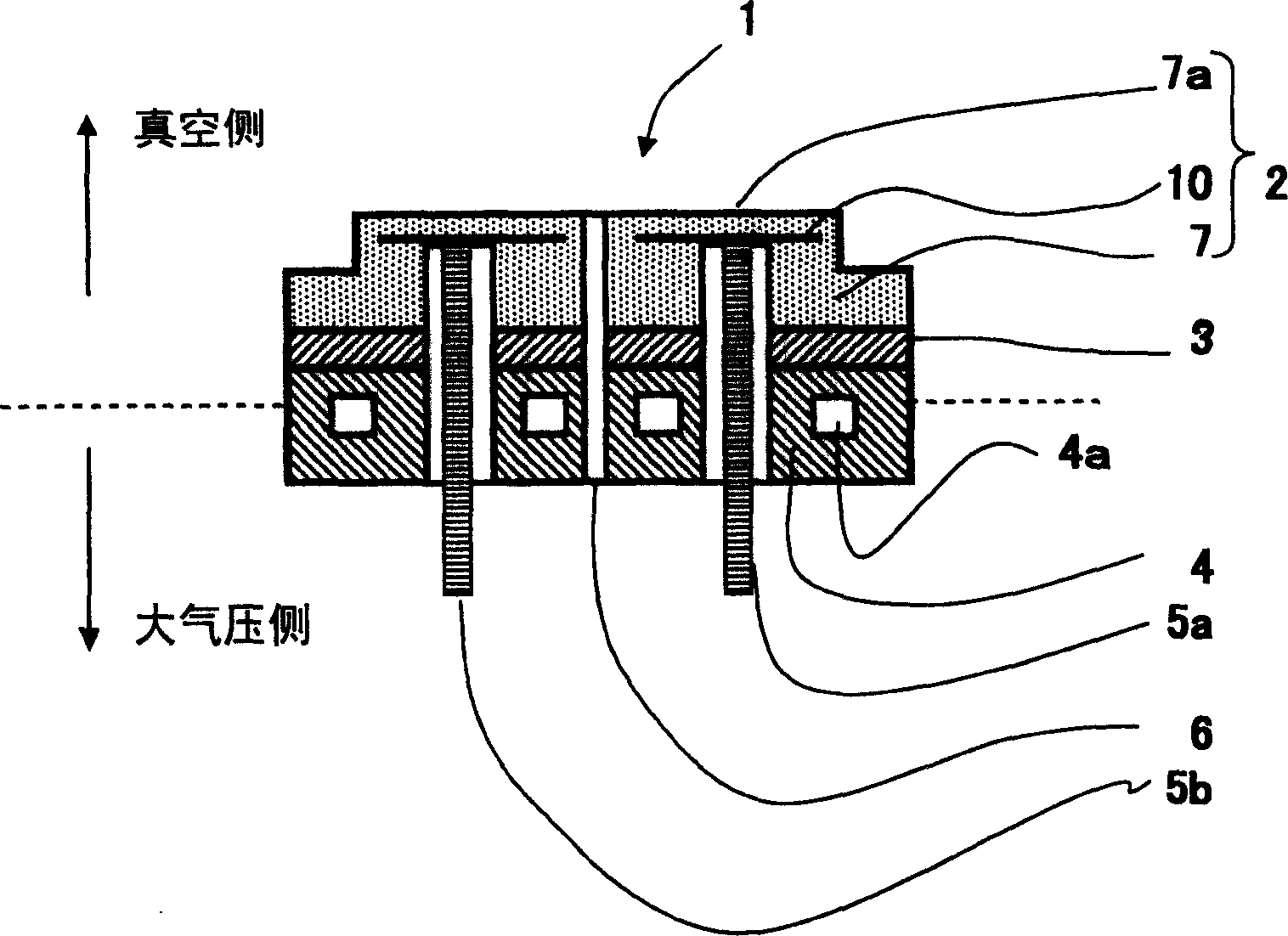
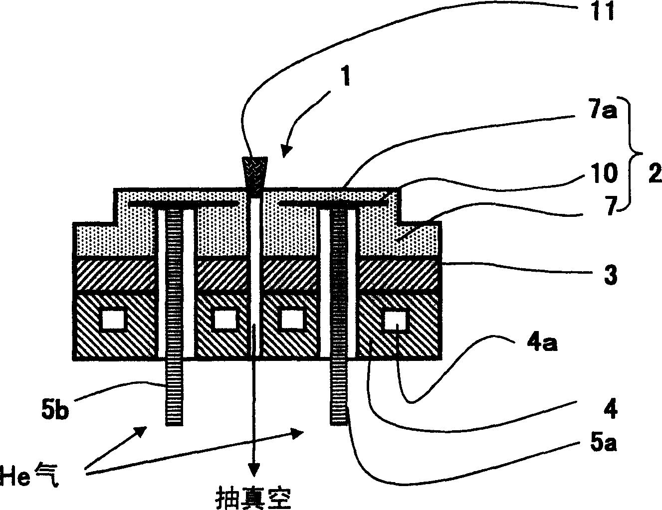
[0069] Figure 1A Is a cross-sectional view showing the first embodiment of the present invention, Figure 1B It is an explanatory diagram showing the leakage rate measurement method.
[0070] The wafer holding member 1 is provided with a wafer holding portion 2 having an electrode 10 on the other major surface or inside of the plate-shaped base 7 as a mounting surface 7a on which a wafer is placed on one main surface of the plate-shaped base 7, and Made of SiC, SiO 2 A plate 4 composed of at least one of Al or Si is joined to the wafer holding portion 2 and the plate 4 on the opposite side surface of the mounting surface 7a of the wafer holding portion 2 using a metal bonding material 3.
[0071] The plate-shaped base 7 is preferably composed of oxide ceramics such as alumina and ceramic materials such as nitrides and carbides. A groove (not shown in the figure) is formed on the mounting surface 7a, and the gas introduction hole 6 penetrates the holding portion 2 Argon gas or th...
Embodiment approach 2
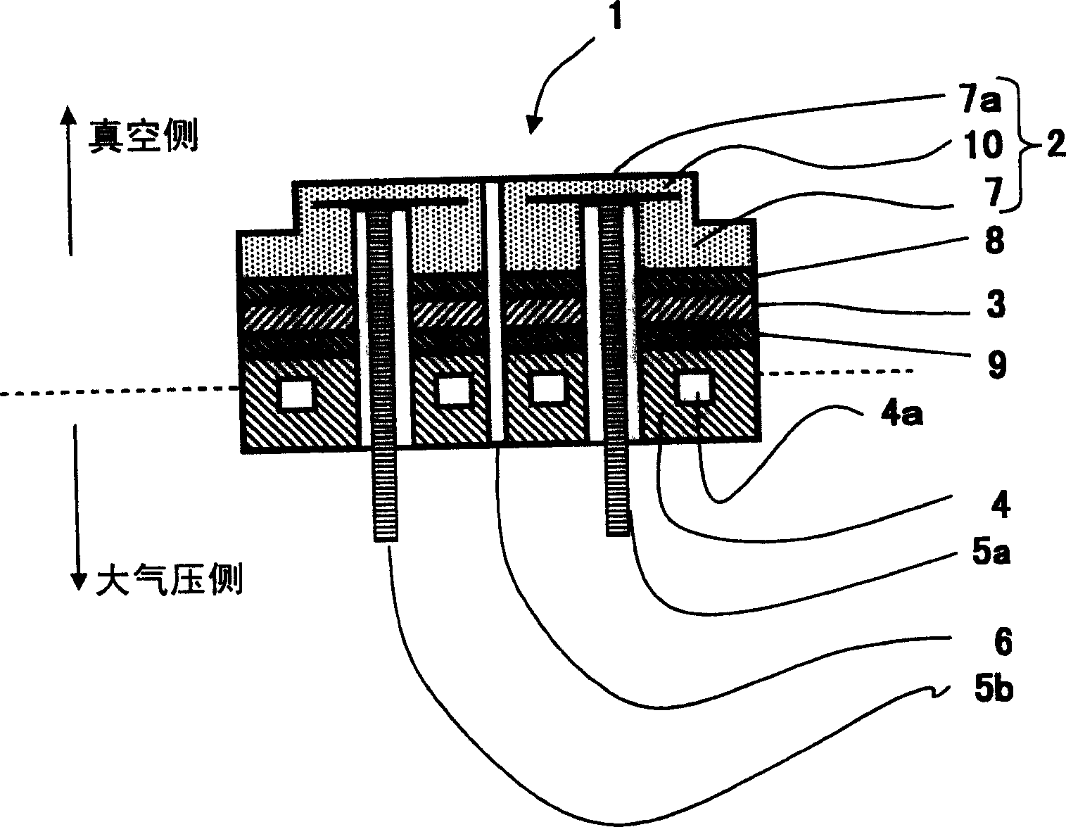
[0111] figure 2 Is a cross-sectional view showing the second embodiment of the present invention, image 3 Is its top view.
[0112] The wafer holding member 1 includes one main surface of the plate-shaped ceramic body 7 as a mounting surface 7a on which the wafer is placed, and a wafer holding portion 2 provided with an electrode 10 on the other main surface or inside of the plate-shaped ceramic body 7 , And the composite material plate 4 containing SiC, Al and Si, provided with a metal layer 8 on the opposite side of the mounting surface 7a of the wafer holding portion 2 and a metal layer 9 on the surface of the pot composite material plate 4, with The two kinds of metal layers 8 and 9 and the metal bonding material 3 are bonded to the wafer holding portion 2 and the plate 4.
[0113]The plate-shaped ceramic body 7 is preferably composed of oxide ceramics such as alumina and ceramics such as nitrides and carbides. A groove (not shown in the figure) is formed on the mounting su...
Embodiment 1
[0148] A molten solidified body of 74% by weight of SiC, 15.6% by weight of Al and 10.4% by weight of Si, a molten solidified body of 84.4% by weight of SiC, 15.6% by weight of Al and 0% by weight of Si, and 89.6% by weight of SiC, Al 0 by weight and Si 10.4 were prepared. Weight% of the melted and solidified body, and then change the immersion time of each melted and solidified body in ethyl silicate to produce SiO 2 Composite materials with varying content. The size of the composite material is 50×50×5mm.
[0149] Then the He leakage rate was measured. The method for measuring the He leakage rate is to polish the surface of the above composite material to Ra 0.1 ~ 0.2 micron with 5 micron diamond, then press the metal cylinder containing an O-ring with an inner diameter of 30 mm and an outer diameter of 34 mm on the composite material On the surface of the tube, under the state of vacuum in the cylinder, put it into a vinylon bag or a box of the desired shape to fill it with hel...
PUM
| Property | Measurement | Unit |
|---|---|---|
| electrical resistivity | aaaaa | aaaaa |
| thermal conductivity | aaaaa | aaaaa |
| thermal conductivity | aaaaa | aaaaa |
Abstract
Description
Claims
Application Information