

Topside active optical device apparatus and method
A technology of optical devices and top surfaces, which is applied to laser parts, structure/shape of optical resonators, lasers, etc., can solve problems such as difficulties, unpopularity, complexity, etc., to improve product life, increase total output, The effect of cost reduction
- Summary
- Abstract
- Description
- Claims
- Application Information
AI Technical Summary
Problems solved by technology
Method used
Image

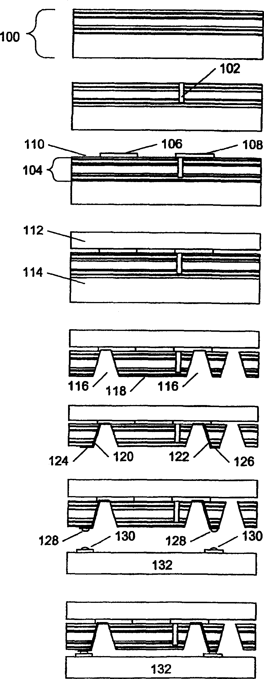
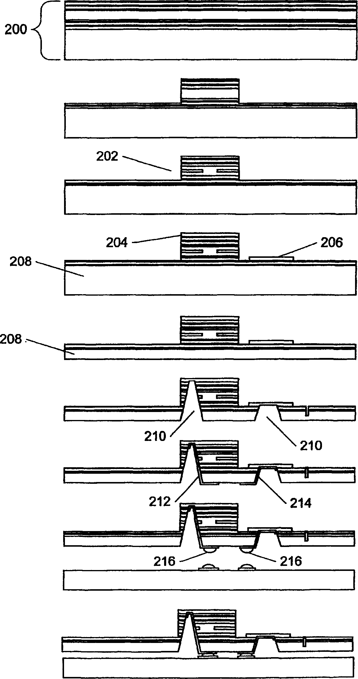
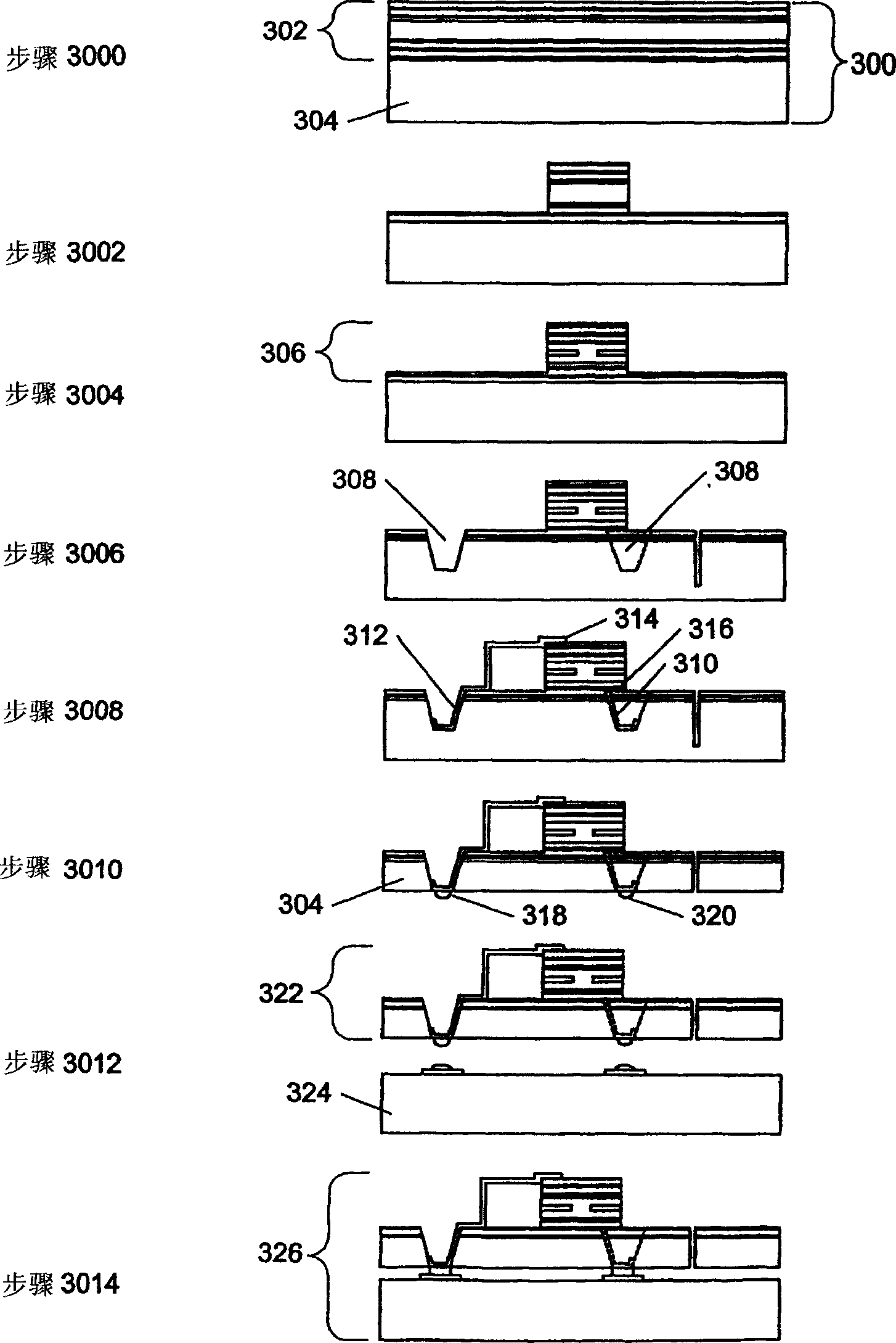
Examples
example 1
[0262] In this example, the process part, the combination of joining materials (such as solder metal), melting point and attachment temperature are shown in Table 4:
[0263]
craft
Material
Material
attach
temperature
Attaching Optics to Electronic ICs
20%Au / 80%Sn
280℃
310℃
Attach the IC to the package
95%Sn / 5%Sb
240℃
270℃
Attaching the package to the printed circuit board
63%Sn / 37%Pb
180℃
210℃
[0264]In this example, the first part of the process begins with the attachment of the optics to the integrated circuit (IC). This is done with the material with the highest melting point (in this case Au20% / Sn80% with a melting point of 280° C.). The interconnected joints are brought together and the temperature is raised above the melting point to melt the solder. The components to be joined are then cooled below the melting point to allow the s...
example 2
[0269] In this example, a similar transceiver is fabricated using a similar process, except that two optical chips (i.e., a laser chip and a photodetector chip) share a common chip and use a thermally active non-conductive melting temperature of 230°C and a curing temperature of 230°C. °C glue attaches an additional component used to align optical fibers and optics beyond the electronic chip. As a result the process is changed so that the attachment step of the components requiring adhesive is performed before the module is attached to the printed circuit board. The steps and materials included in the process are shown in Table 5.
[0270] craft
Material
material melting point
Attachment temperature
Attaching Optical IC to Electronic IC
20%Au / 80%Sn
280℃
310℃
Attach the IC to the package
95%Sn / 5%Sb
240℃
260℃
Attaching the Alignment Sheet to the Package
hot glue
230℃
230℃
Attaching the pa...
PUM
 Abstract
Description
Claims
Application Information