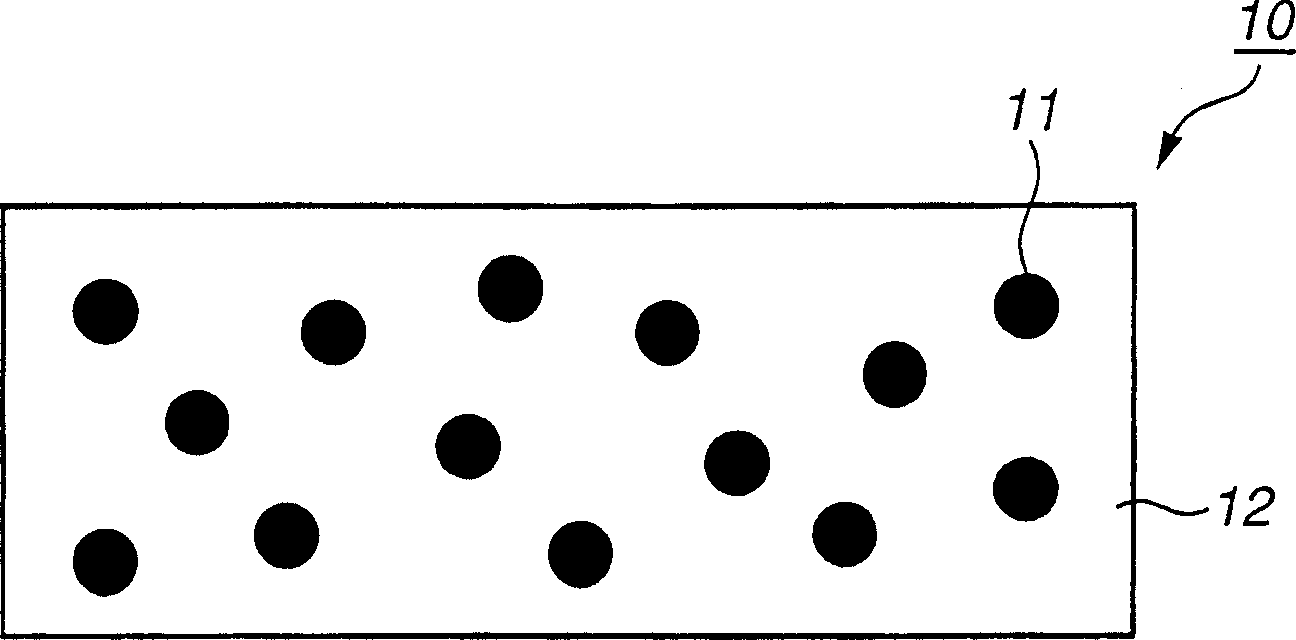
Printed circuit board
A technology of magnetic nanoparticles and insulators, applied in the direction of printed circuits, circuits, electrical components, etc., can solve the problems of low mechanical strength, unusable use, restrictions, etc., and achieve the effect of low transmission loss
- Summary
- Abstract
- Description
- Claims
- Application Information
AI Technical Summary
Problems solved by technology
Method used
Image

Examples
Embodiment 1
[0094] Materials used in Embodiment 1, a method of forming a PCB, and a method of forming a transmission line will be described below.
[0095] (1) Materials used
[0096] (i) Magnetic nanoparticles: using Fe covered with oleic acid synthesized by alcohol reduction method 3 o 4 Toluene dispersion of magnetic nanoparticles. Fe 3 o 4 The average particle size of the magnetic nanoparticles is 16 nm. The standard deviation of the particle size distribution is 19% of the mean particle size.
[0097] (ii) Insulator material: Powdered polytetrafluoroethylene (average particle size: 25 μm) is used
[0098] (2) Formation method of PCB
[0099] Powdered PTFE mixed into Fe 3 o 4 magnetic nanoparticles in toluene dispersion. Among them, Fe 3 o 4 The volume ratio of magnetic nanoparticles to polytetrafluoroethylene was set at 30:70.
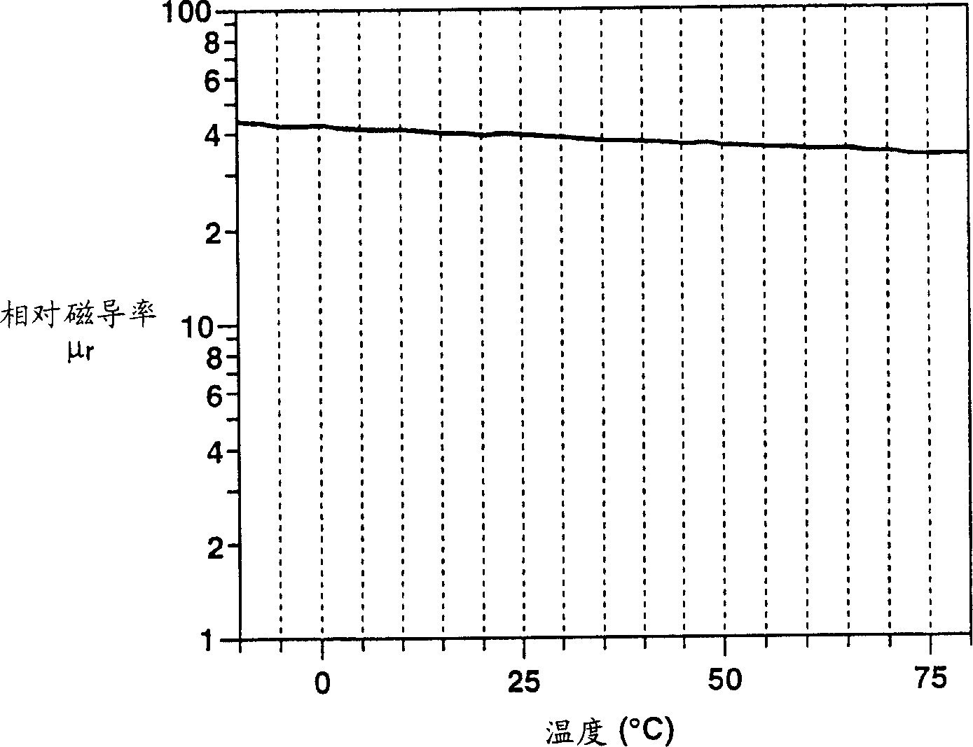
[0100] Then, the solution was kept at 60°C and the toluene was evaporated by stirring the solution using a high speed stirrer to obtain a black ...
Embodiment 2
[0110] Materials used in Embodiment 2, a method of forming a PCB, and a method of forming a transmission line will be described below.
[0111] (1) Materials used
[0112] (i) Magnetic nanoparticles: A toluene dispersion of oleic acid-covered Mn—Zn ferrite nanoparticles synthesized by an alcohol reduction method was used. The average particle diameter of the Mn-Zn ferrite nanoparticles is 10 nm. The standard deviation of the particle size distribution is 29% of the mean particle size.
[0113] (ii) Insulator material: Powdered polytetrafluoroethylene (average particle size: 25 μm) is used
[0114] (2) Formation method of PCB
[0115] Mix powdered PTFE into the toluene dispersion of Mn-Zn ferrite nanoparticles. Wherein, the volume ratio of Mn-Zn ferrite nanoparticles to polytetrafluoroethylene is set to 40:60.
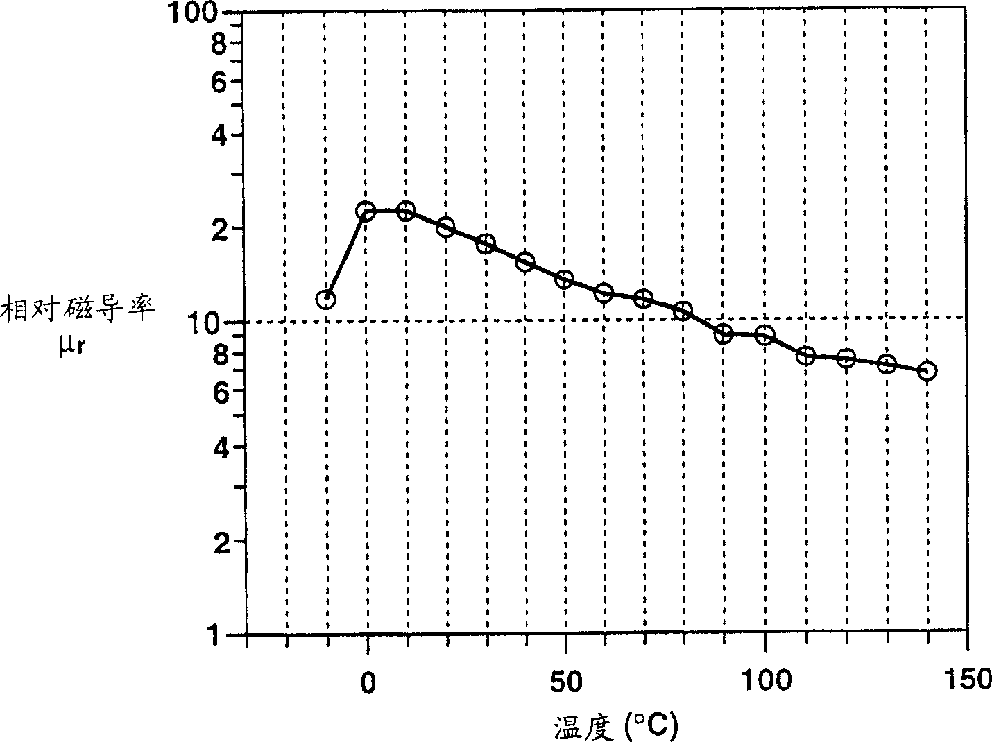
[0116] Then, the solution was kept at 60°C and the toluene was evaporated by stirring the solution using a high speed stirrer to obtain a black residual solid mate...
Embodiment 3
[0123] Materials used in Embodiment 3, a method of forming a PCB, and a method of forming a transmission line will be described below.
[0124] (1) Materials used
[0125] (i) Magnetic nanoparticles: using Fe covered with oleic acid synthesized by pyrolysis 50 co 50 Dispersion of nanoparticles in toluene. Fe 50 co 50 The average particle size of the nanoparticles is 12 nm. The standard deviation of the particle size distribution is 17% of the mean particle size.
[0126] (ii) Insulator material: Powdered polytetrafluoroethylene (average particle size: 25 μm) is used
[0127] (2) Formation method of PCB
[0128] Mix powdered PTFE in Fe 50 co 50 nanoparticles in toluene dispersion. Among them, Fe 50 co 50 The volume ratio of nanoparticles to polytetrafluoroethylene was set at 20:80.
[0129] Then, the solution was kept at 60°C and the toluene was evaporated by stirring the solution using a high speed stirrer to obtain a black residual solid material.
[0130] Then,...
PUM
| Property | Measurement | Unit |
|---|---|---|
| The average particle size | aaaaa | aaaaa |
| The average particle size | aaaaa | aaaaa |
| The average particle size | aaaaa | aaaaa |
Abstract
Description
Claims
Application Information