Strained FinFET CMOS device structures

A device structure, semiconductor technology, applied in the direction of semiconductor devices, semiconductor/solid-state device manufacturing, transistors, etc.

Inactive Publication Date: 2005-11-09
GLOBALFOUNDRIES INC
View PDF2 Cites 31 Cited by
  • Summary
  • Abstract
  • Description
  • Claims
  • Application Information

AI Technical Summary

Problems solved by technology

This prior art approach is aimed at improving nFET mobility and thus only achieves limited improvements in CMOS circuits

Method used


Image

  • Strained FinFET CMOS device structures
  • Strained FinFET CMOS device structures
  • Strained FinFET CMOS device structures

Examples


Embodiment Construction

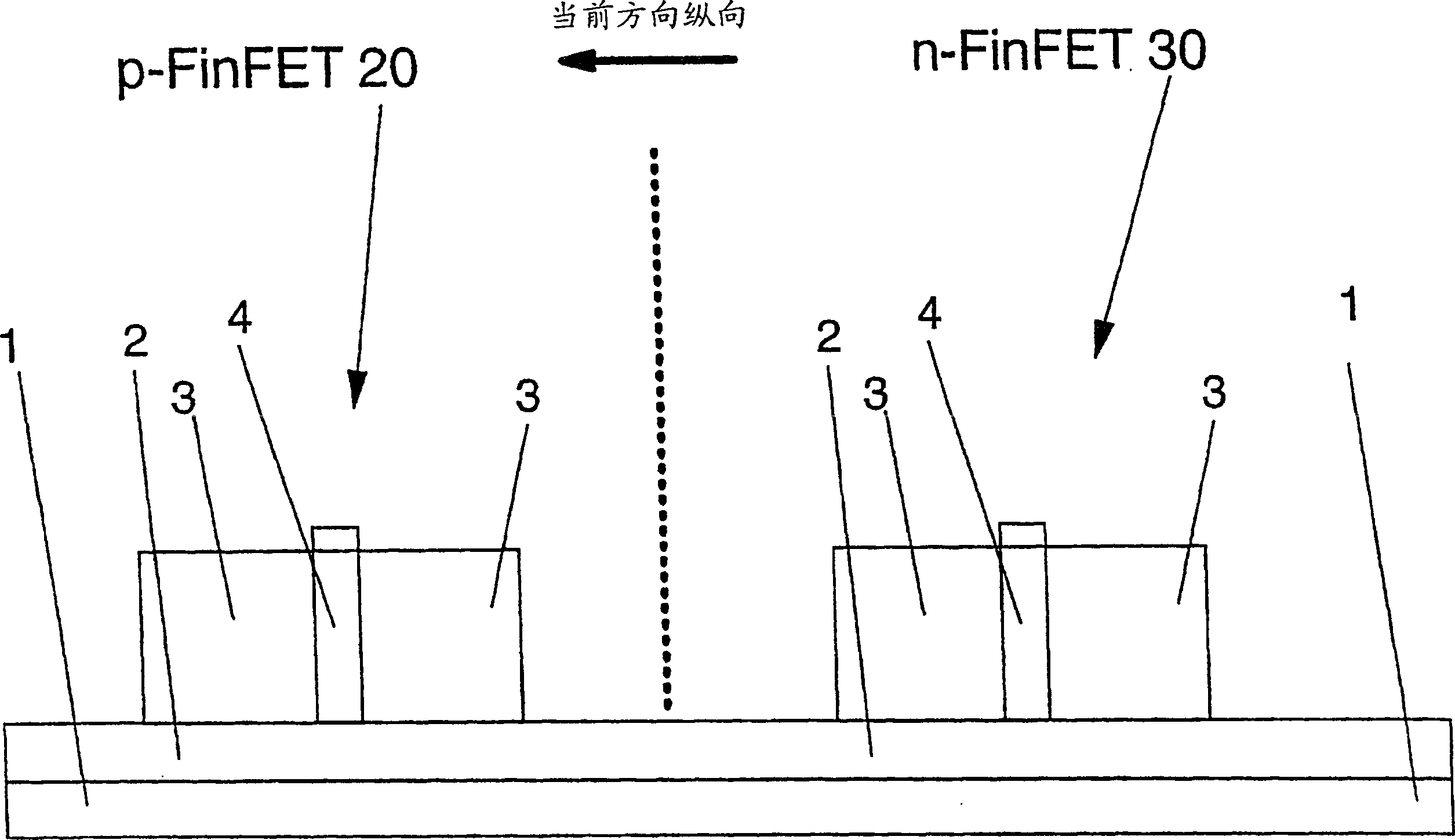
[0015] The invention aims to provide a novel FinFET semiconductor device structure and a manufacturing method thereof. A preferred final structure according to the invention is shown in Figure 16 , 17 middle.

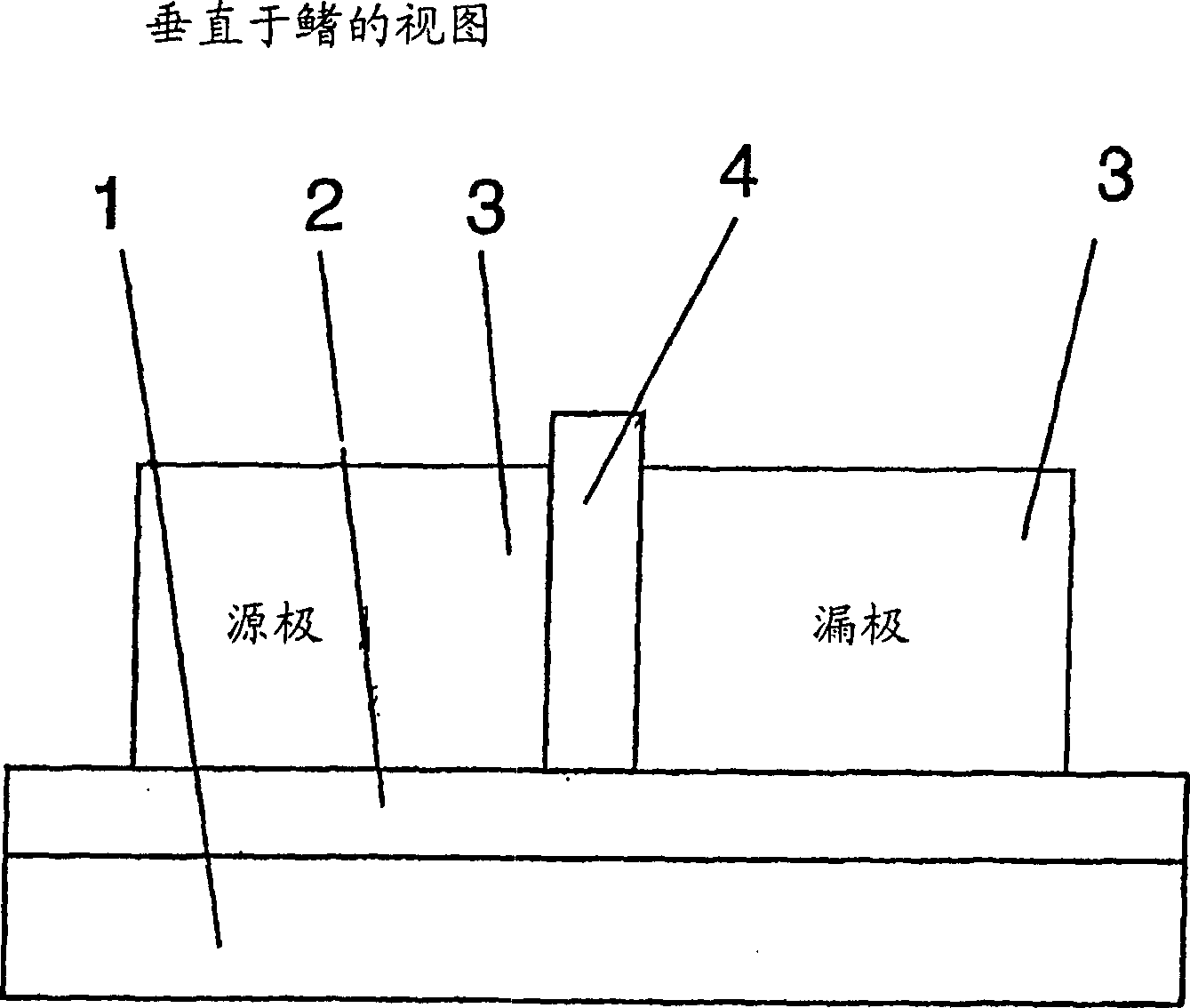
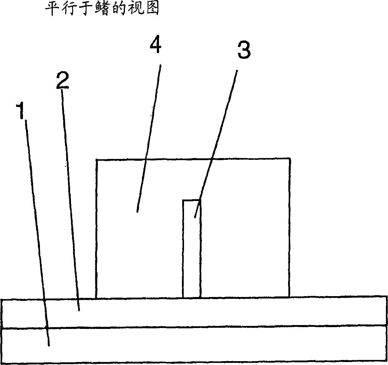
[0016] Referring now to the remaining figures, in particular Figures 1 to 3, a known FinFET device (Figures 1, 2) and device structure (Figure 3) is shown.

[0017] First, standard or conventional FinFET device fabrication processes are performed: patterning and etching fins; forming gate dielectric and conductors, sidewall spacers (not shown); doping source / drains; and salicide ( salicide). After salicide, the gate sidewall spacers are removed to facilitate the processing that will induce strain in the fins according to the present invention.

[0018] More specifically, as described with reference to FIG. 3 , for example, an SOI wafer is provided. The SOI wafer consists of a SiO 2 The substrate 1 under the buried layer 2 is shown in FIG. 3 . In SiO 2 Above the...


PUM


Abstract

A semiconductor device structure, includes a PMOS device and an NMOS device disposed on a substrate the PMOS device including a compressive layer stressing an active region of the PMOS device, the NMOS device including a tensile layer stressing an active region of the NMOS device, wherein the compressive layer includes a first dielectric material, the tensile layer includes a second dielectric material, and the PMOS and NMOS devices are FinFET devices.

Description

technical field [0001] The invention relates to a double-gate semiconductor device structure, in particular to a FinFET device. Background technique [0002] Due to the ability to obtain near-ideal sub-threshold slope, absence of body effect, freedom from short-channel effect, and very high current drive capability, the double-gate semiconductor device structure is a promising future generation of microelectronic devices. s Choice. [0003] A technology-related dual-gate device structure is the Fin Field Effect Transistor (FinFET). FinFETs are particularly attractive due to their relative simplicity of fabrication compared to other dual-gate devices. The channels used in FinFETs are thin rectangular Si islands, often called fins. The gate wraps around the fin so that the channel is gated on both sides of the vertical portion of the fin structure, providing gate control over planar single gate MOSFETs. [0004] FinFETs are well known. For example, U.S. Patent No. 6,413,8...

Claims


Application Information

Patent Timeline
Patent Type & Authority Applications(China)
IPC IPC(8): H01L21/00H01L21/336H01L21/8238H01L27/092H01L27/12H01L29/786
CPCH01L21/823807H01L27/092H01L29/7843H01L29/7842H01L21/823828H01L29/66795H01L29/785H01L27/1203
Inventor 布鲁斯·B·多丽丝杜里塞蒂·奇达姆巴拉奥米凯·耶翁杰克·A·曼德尔曼
Owner GLOBALFOUNDRIES INC
Why Eureka
Try Eureka