Manufacturing apparatus and method for large-scale production of thin-film solar cells

A technology of solar cells and conductive films, applied in the fields of final product manufacturing, sustainable manufacturing/processing, semiconductor/solid-state device manufacturing, etc.

Inactive Publication Date: 2005-11-30
BEIJING APOLLO DING RONG SOLAR TECH
View PDF7 Cites 23 Cited by
  • Summary
  • Abstract
  • Description
  • Claims
  • Application Information

AI Technical Summary

Problems solved by technology

[0020] In U.S. Patent 5,986,204 ('204) Iwasaki et al. present a solution to the problems associated with conventional CIGS solar cells

Method used


Image

  • Manufacturing apparatus and method for large-scale production of thin-film solar cells
  • Manufacturing apparatus and method for large-scale production of thin-film solar cells
  • Manufacturing apparatus and method for large-scale production of thin-film solar cells

Examples


Embodiment Construction

[0055] Now, the present invention will be described and compared with the structure of a conventional prior art CIGS solar cell. A new cell structure and fabrication process will be detailed for a modular roll-to-roll sputter deposition system specifically designed to provide optimal realization of the process.

[0056] It should be noted that, as used herein, the terms "over" and "on" both inherently include "directly on.. ..." (without intervening materials, elements, or spaces disposed therebetween), and "indirectly over" (intermediate materials, elements, or spaces disposed therebetween). For example, forming a unit "on a substrate" may include directly forming a unit on a substrate without intermediate materials / units therebetween, and may also include indirectly forming a unit on a substrate with one or more intermediate materials / units therebetween.

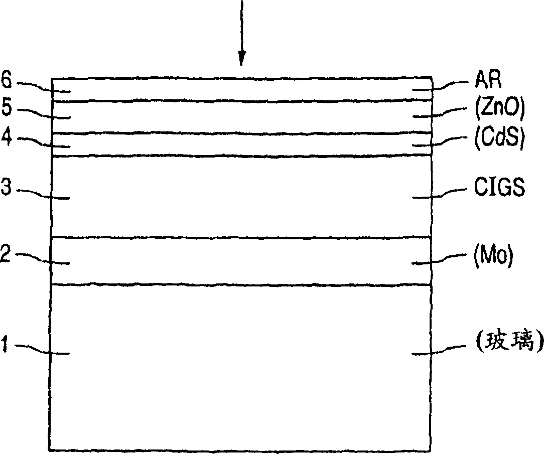
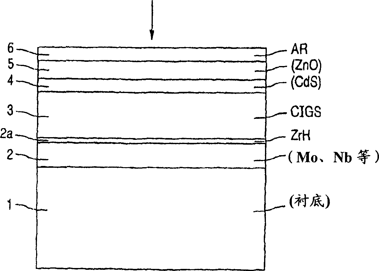
[0057] Figure 6 A simplest embodiment of a basic solar cell according to the invention comprising a barrier layer of ...


PUM

PropertyMeasurementUnit
widthaaaaaaaaaa
thicknessaaaaaaaaaa
thicknessaaaaaaaaaa

Abstract

A method of manufacturing improved thin-film solar cells entirely by sputtering includes a high efficiency back contact/reflecting multi-layer containing at least one barrier layer consisting of a transition metal nitride. A copper indium gallium diselenide (Cu(InxGa1-x)Se2) absorber layer (X ranging from 1 to approximately 0.1) is co-sputtered from specially prepared electrically conductive targets using dual cylindrical rotary magnetron technology. The band gap of the absorber layer can be graded by varying the gallium content, and by replacing the gallium partially or totally with aluminum. Alternately the absorber layer is reactively sputtered from metal alloy targets in the presence of hydrogen selenide gas. RF sputtering is used to deposit a non-cadmium containing window layer of ZnS. The top transparent electrode is reactively sputtered aluminum doped ZnO. A unique modular vacuum roll-to-roll sputtering machine is described. The machine is adapted to incorporate dual cylindrical rotary magnetron technology to manufacture the improved solar cell material in a single pass.

Description

[0001] This application claims the benefit of US Provisional Application 60 / 415009, filed September 30, 2002 and US Provisional Application 60 / 435814, filed December 19, 2002. technical field [0002] The invention disclosed herein relates generally to the field of optoelectronics, and more particularly to the only highly light-transmitting optical fiber for the manufacture of thin-film solar cells based on an absorber layer comprising copper, indium, gallium, aluminum and selenium and having a polycrystalline chalcopyrite structure. Rate roll in and out vacuum deposition system and method. Background technique [0003] In recent years, interest in thin film optoelectronics has developed. This is mainly due to the improved conversion efficiency of cells manufactured at laboratory scale and the effective reduction of manufacturing costs compared to earlier and more expensive crystalline and polysilicon technologies. The term "thin film" is used to distinguish this type of so...

Claims


Application Information

Patent Timeline
Patent Type & Authority Applications(China)
IPC IPC(8): B22F3/00H01L31/032H01L31/108
CPCY02E10/50Y02P70/50
Inventor D·R·霍拉斯
Owner BEIJING APOLLO DING RONG SOLAR TECH
Why Eureka
Try Eureka