Epitaxial wafer for semiconductor light-emitting device and semiconductor light-emitting device

A technology of light-emitting devices and semiconductors, which is applied in the direction of semiconductor devices, semiconductor lasers, laser components, etc., can solve the problems of device characteristics and reliability degradation, and achieve the effect of inhibiting and reducing diffusion

Inactive Publication Date: 2005-12-07
HITACHI CABLE
View PDF2 Cites 3 Cited by
  • Summary
  • Abstract
  • Description
  • Claims
  • Application Information

AI Technical Summary

Problems solved by technology

[0004] However, when Zn is doped at a high concentration, Zn will diffuse into the active layer during t

Method used


Image

  • Epitaxial wafer for semiconductor light-emitting device and semiconductor light-emitting device
  • Epitaxial wafer for semiconductor light-emitting device and semiconductor light-emitting device
  • Epitaxial wafer for semiconductor light-emitting device and semiconductor light-emitting device

Examples


Embodiment 1

[0039] Next, examples of the present invention will be described.

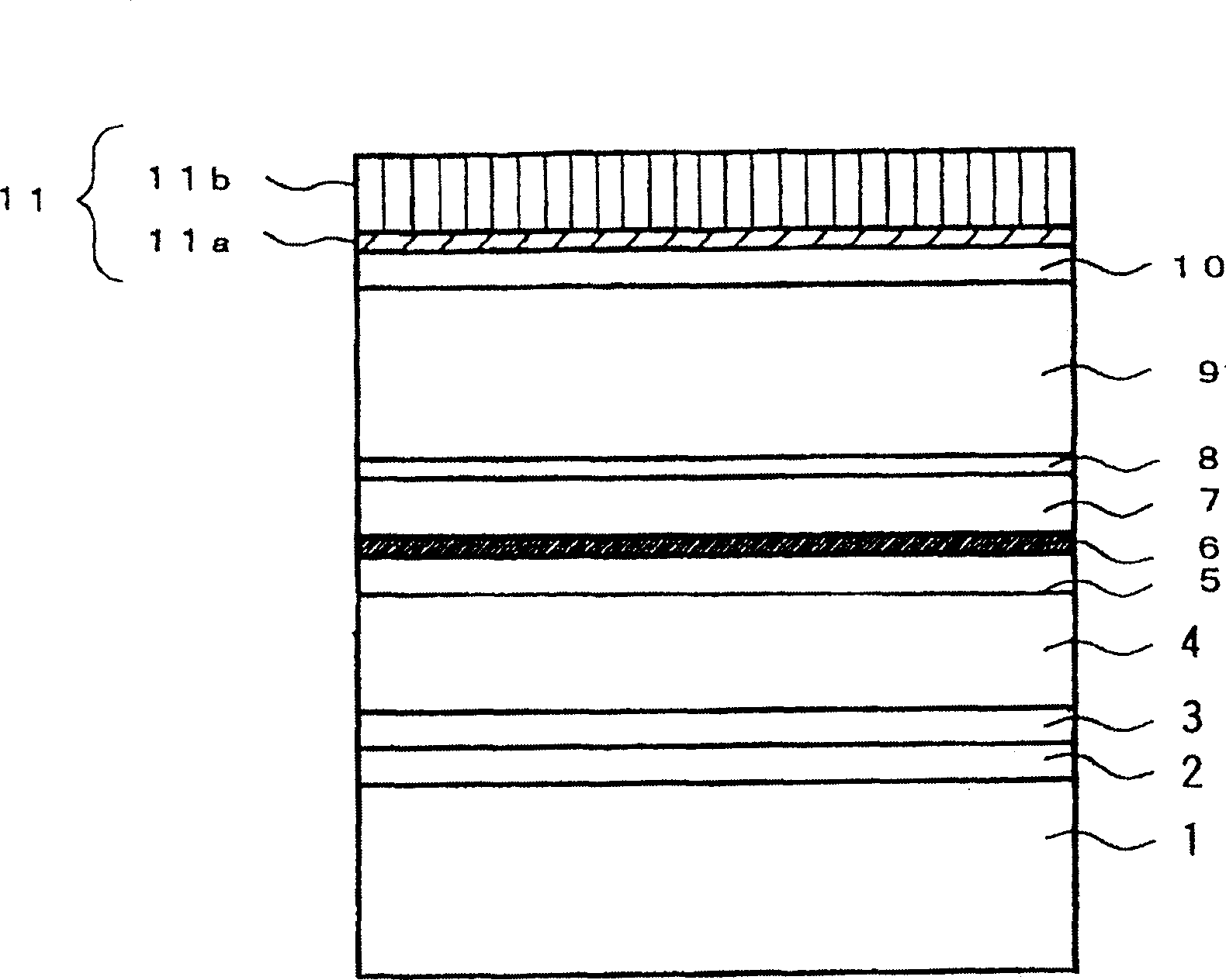
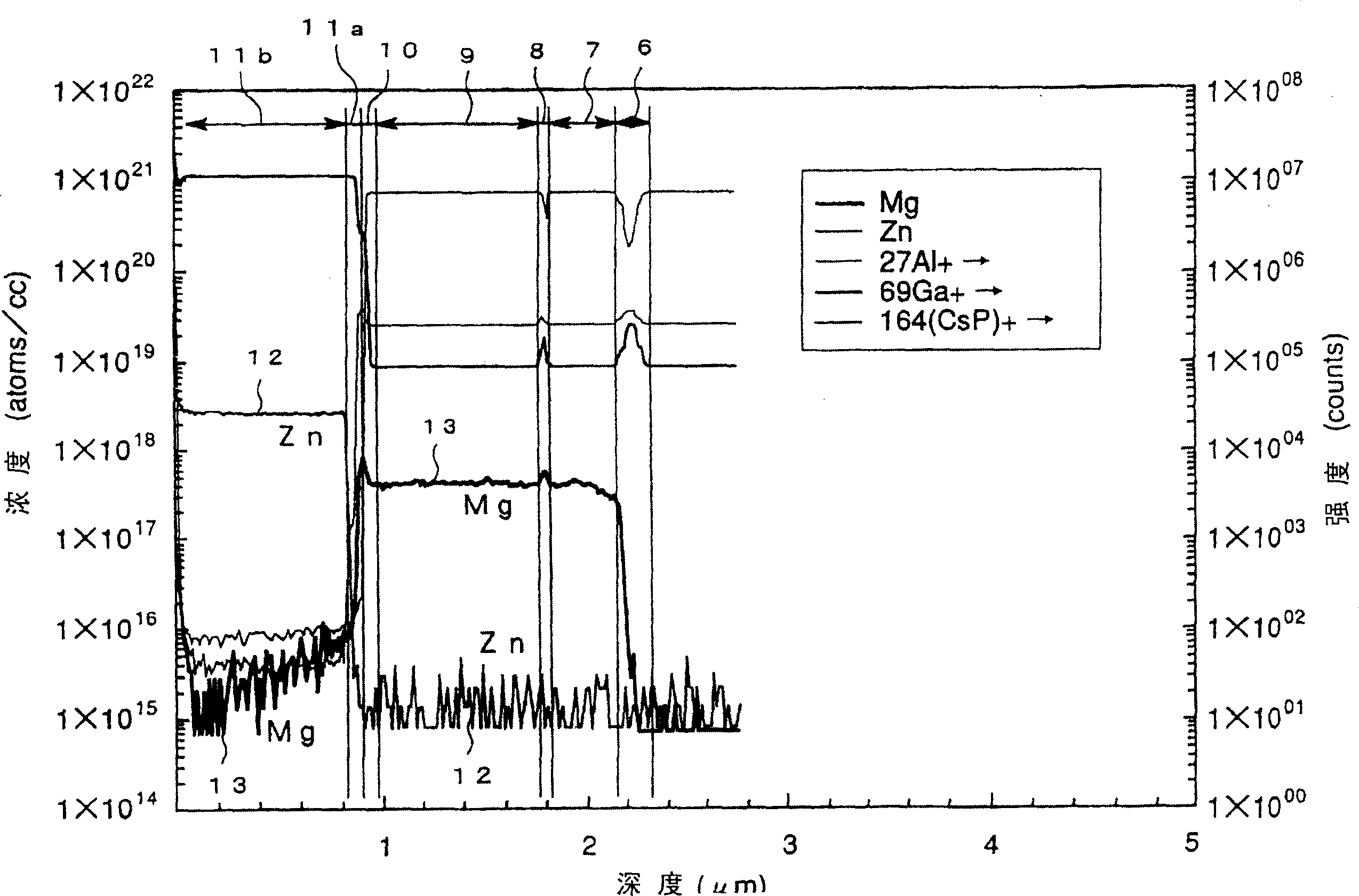
[0040] like figure 1 As shown, on an n-type substrate 1 composed of GaAs, an n-type buffer layer 2 composed of GaAs, an n-type buffer layer 3 composed of GaInP lattice-matched to it, and an n-type buffer layer 3 composed of (Al 0.7 Ga 0.3 ) 0.5 In 0.5 The n-type cladding layer 4 composed of P, on which, is grown sequentially by (Al 0.5 Ga 0.5 ) 0.5 In 0.5 An undoped guide layer 5 composed of P, an active layer 6 composed of a multi-quantum well (MQW) composed of a barrier layer and a strained GaInP well layer, and then composed of (Al 0.7 Ga 0.3 ) 0.5 In 0.5 The Mg-doped p-type first cladding layer 7 composed of P, the p-type etching stop layer 8 composed of GaInP, and the (Al 0.7 Ga 0.3 ) 0.5 In 0.5 The Mg-doped p-type second cladding layer 9 made of P, and the Mg-doped p-type intermediate layer 10 made of GaInP.

[0041] In this way, the Mg-doped p-type cladding layer (Mg-doped layer) 11a made...

Embodiment 2

[0046] In the zinc diffusion suppressing layer (Mg-doped p-type cladding layer 11a) of the present invention, the doping amount of magnesium can be freely set to some extent. Therefore, as another example, the carrier concentration of the Mg-doped p-type cladding layer (Mg-doped layer) 11a as the zinc diffusion suppressing layer is set to 4×10 18 cm -3 , the Zn-doped p-type cladding layer (layer doped with Zn) 11b is also set as 4×10 18 cm -3 To form the result, the same effect can be exerted.

Embodiment 3

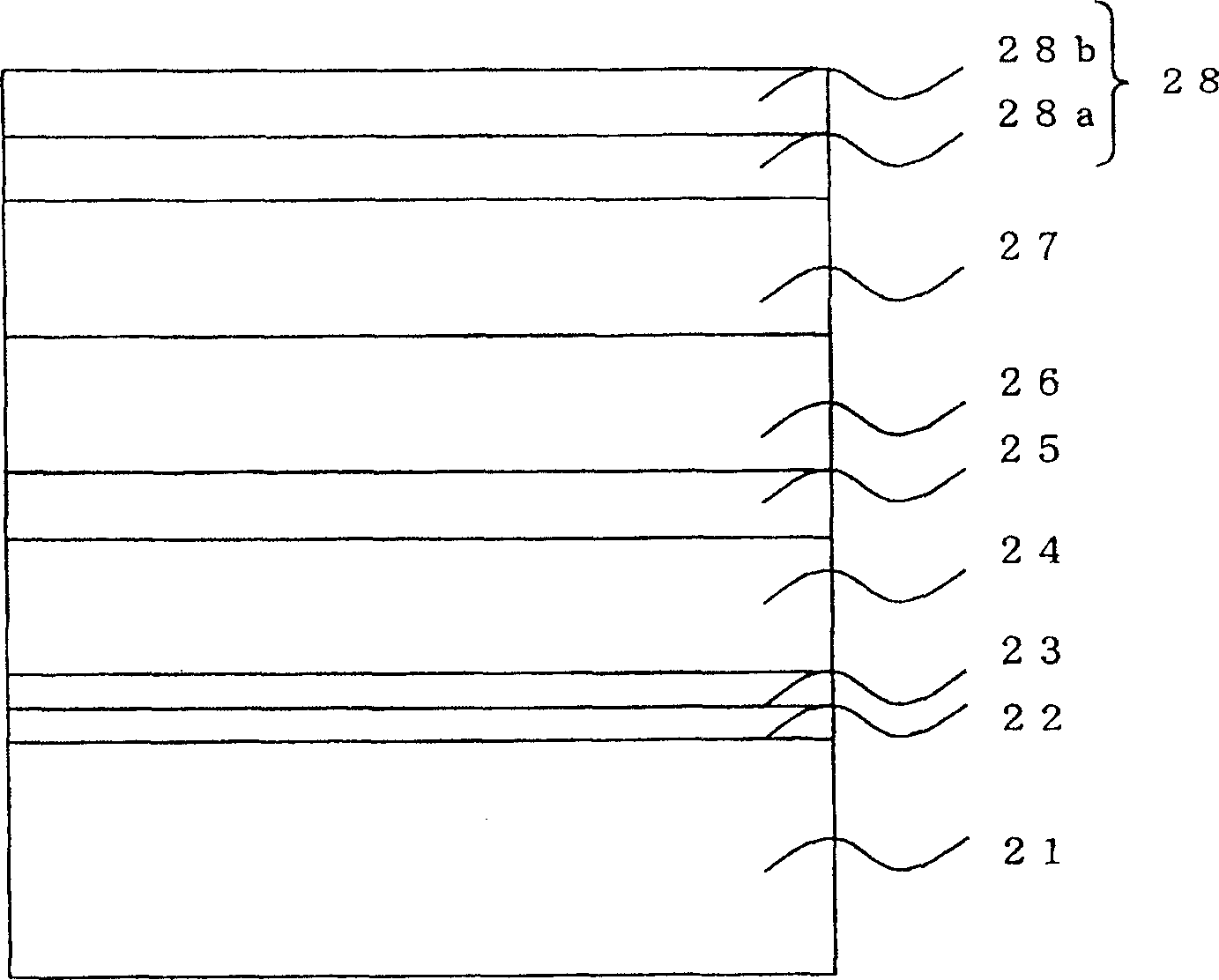
[0048] like image 3 As shown, on the n-type substrate 21 made of GaAs, the n-type buffer layer 22 made of GaAs is epitaxially grown sequentially, and the n-type buffer layer 22 made of Al 0.5 Ga 0. The n-type DBR layer 23 composed of a thin film multilayer structure of 5As and AlAs, composed of (Al 0.7 Ga 0.3 ) 0.5 In 0.5 An n-type cladding layer 24 composed of P, on which, an active layer 25 composed of a multi-quantum well (MQW) composed of a barrier layer and a strained GaInP well layer is grown sequentially, consisting of (Al 0.7 Ga 0.3 ) 0.5 In 0.5 The Mg-doped p-type cladding layer 26 made of P, and the p-type current diffusion layer 27 made of GaP.

[0049] In this way, the Mg-doped p-type cladding layer (Mg-doped layer) 28a made of GaAs and the Zn-doped p-type clad layer made of GaAs are grown sequentially on the uppermost part with the zinc diffusion suppressing layer of the present invention. Covering layer (Zn-doped layer) 28b. The thickness of the Mg-dop...


PUM

PropertyMeasurementUnit
Thicknessaaaaaaaaaa
Carrier concentrationaaaaaaaaaa
Thicknessaaaaaaaaaa

Abstract

The present invention provided an epitaxial wafer for a light-emitting element in which Zn in a p-type cap layer, consisting of GaAs, is prevented from being diffused into a cladding layer and an active layer, and thereby to provide a light-emitting element by which stable high output operation and high temperature operation can be performed and high reliability LED and LD can be obtained. In the epitaxial wafer for the semiconductor light-emitting element in which at least an n-type clad layer 4, an active layer 6, p-type clad layers 7, 9, and a p-type cap layer 11 are sequentially laminated on an n-type substrate 1, and p-type dopant of the p-type clad layers 7, 9 is Mg, the p-type cap layer 11 consists of at least two layers, i.e. a Mg-doped layer 11a dna a Zn-doped layer 11b, sequentially formed from the substrate side.

Description

technical field [0001] The present invention relates to epitaxial wafers for semiconductor light-emitting devices (light-emitting diodes, semiconductor lasers), in particular to epitaxial wafers for semiconductor light-emitting devices suitable for aluminum gallium indium phosphide (AlGaInP)-based light-emitting devices using magnesium (Mg) as a P-type dopant sheet, and semiconductor light-emitting devices made using it. Background technique [0002] In AlGaInP-based crystal growth for semiconductor light-emitting devices using the metalorganic vapor phase growth (MOVPE) method, silicon (Si) and selenium (Se) are generally used as n-type dopants, and zinc (Zn) and magnesium (Mg) as p dopants. type dopant. For semiconductor laser (LD) epitaxial wafers, when Zn is used as the p-type dopant, the carrier concentration of the p-type cladding layer is usually set to 4×10 17 cm -3 Relatively low concentrations of around. [0003] In recent years, among semiconductor lasers, a h...

Claims


Application Information

Patent Timeline
IPC IPC(8): H01L33/14
Inventor 铃木良治大石昭夫
Owner HITACHI CABLE
Why Eureka
Try Eureka