Diode with improved energy impulse rating

A technology of grades and electrode layers, used in diodes, semiconductor/solid-state device components, semiconductor devices, etc., can solve the problems of complex manufacturing and expensive multi-layer structures

Inactive Publication Date: 2006-01-18
TE CONNECTIVITY CORP
View PDF5 Cites 7 Cited by
  • Summary
  • Abstract
  • Description
  • Claims
  • Application Information

AI Technical Summary

Problems solved by technology

Needless to say, for fabrication, these multilayer structures would become very complex and relatively expensive to manufacture

Method used


Image

  • Diode with improved energy impulse rating
  • Diode with improved energy impulse rating
  • Diode with improved energy impulse rating

Examples


Embodiment Construction

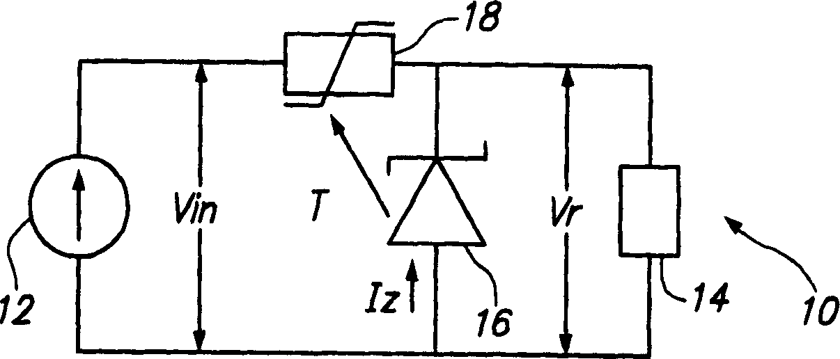
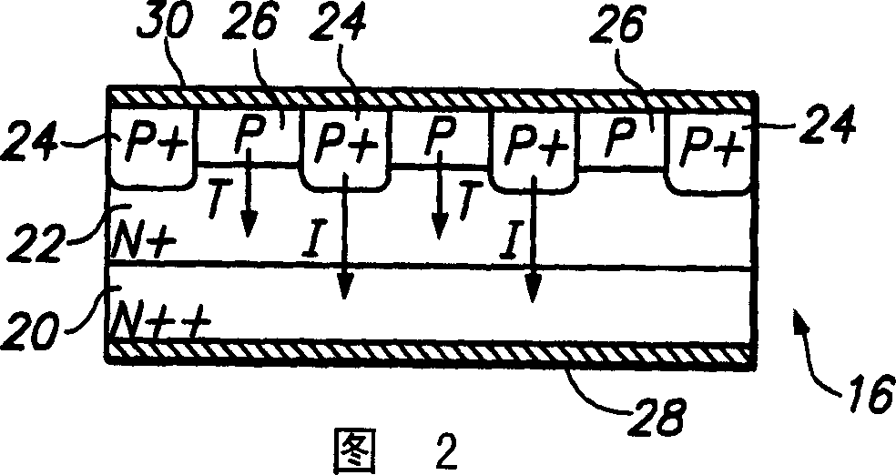
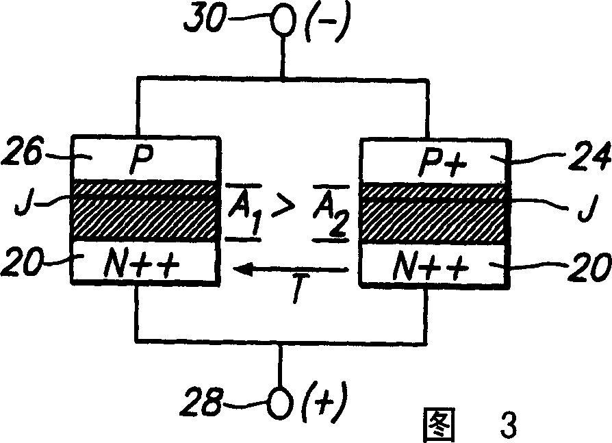
[0031] We have discovered diode chip arrangements and structures that increase the temperature withstand capability of the diode in response to overvoltage energy pulses. The diode includes regions of higher resistivity (eg, p+ regions) created by epitaxial growth or impurity diffusion. Heavier doping is provided in the cell region of the diode (eg p++) to ensure Zener tunneling and / or impact ionization at reverse bias voltage breakdown levels. As the chip temperature increases, the lighter doped (p+) regions reach the intrinsic (ohmic) transition temperature before the more heavily doped (p++) cell regions, whereby a concentrated anode-cathode current flows through These lighter doped regions of the chip. This diversion of current increases the temperature in the more lightly doped regions, thereby spreading the temperature more uniformly in the chip and affecting the ohmic current-voltage characteristics of the more lightly doped regions. The ratio of intrinsic / zener volta...


PUM


Abstract

An energy pulse clamping semiconductor diode (16) includes a substrate (20) having carriers of a first type of conductivity in a first, high concentration level (e.g. n++), a first major face and a second major face opposite to the first major face; a layer of semiconductor material (22) having carriers of the first type of conductivity in a second concentration level lower than the first level (e.g. n+), and having an outer surface; a region (26) formed at an outer surface having carriers of a second type of conductivity in a third concentration level (e.g. p+); at least one cell having carriers of the second type of conductivity in a fourth concentration level greater than the third concentration level (e.g. p++); a cathode electrode (30) and an anode electrode (28). The diode is most preferably included in an overvoltage protection circuit including a PPTC resistor in series with the cathode electrode and thermally coupled to the diode.

Description

technical field [0001] The invention relates to a circuit element. In particular, the invention relates to an overvoltage protection diode that is better able to withstand high energy electrical pulses. Background technique [0002] A semiconductor diode generally refers to a device with two terminals, an anode-cathode. Such diodes typically consist of single crystal p-type doped (positive charge carriers or "holes" and n-type doped (negative charge carriers or electrons) regions formed adjacently in a semiconductor wafer or layer in order to realize p-n junction and constitute.For example, p-type epitaxial layer can be formed on n-type wafer or substrate so that form p-n junction, or n-doped epitaxial layer can be formed on p-doped wafer or substrate to form an n-p junction. [0003] Semiconductor diodes generally exhibit much higher conductivity in one direction of current flow (forward bias) than the other direction (reverse bias). However, for p-n diodes or p-n zener...

Claims


Application Information

Patent Timeline
Patent Type & Authority Applications(China)
IPC IPC(8): H01L29/861H01L23/58H01L21/329H01L21/00H01L29/06H01L29/866
CPCH01L29/866H01L29/0692H01L27/0255H01L29/66106H01L29/66113
Inventor A·科甘栾纪源A·米科拉察克
Owner TE CONNECTIVITY CORP
Why Eureka
Try Eureka