Cooled deposition baffle in high density plasma semiconductor processing

A plasma and baffle technology, used in semiconductor/solid-state device manufacturing, gaseous chemical plating, coating, etc., can solve the problems of destroying devices, increasing pollutants, etc., to reduce pollution, uniform heat flux, and uniform temperature Effect

Inactive Publication Date: 2006-01-18
TOKYO ELECTRON LTD
View PDF6 Cites 17 Cited by
  • Summary
  • Abstract
  • Description
  • Claims
  • Application Information

AI Technical Summary

Problems solved by technology

This thermal stress leads to spalling of the coating and generation of particles, which add contamination to the process and damage devices formed on the semiconductor substrate

Method used


Image

  • Cooled deposition baffle in high density plasma semiconductor processing
  • Cooled deposition baffle in high density plasma semiconductor processing
  • Cooled deposition baffle in high density plasma semiconductor processing

Examples


Embodiment Construction

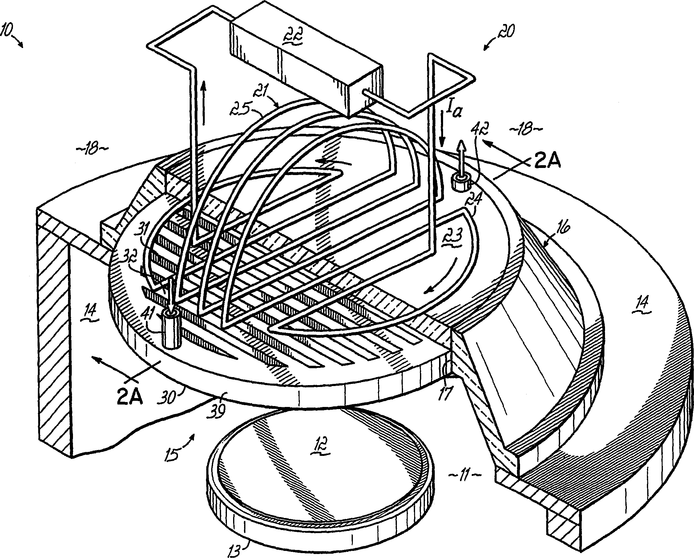
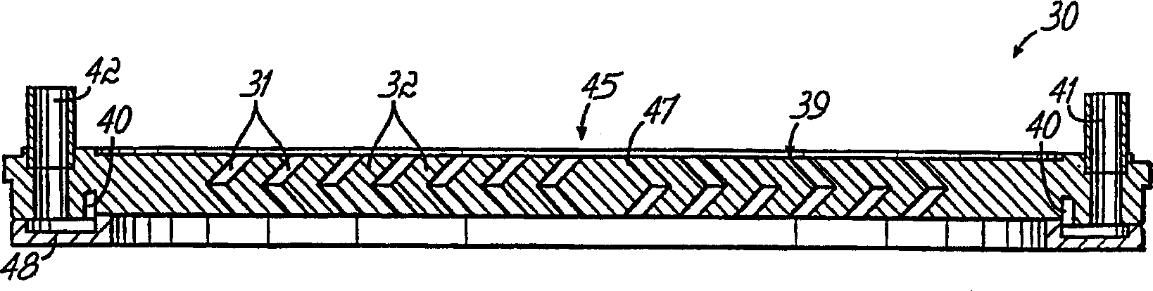
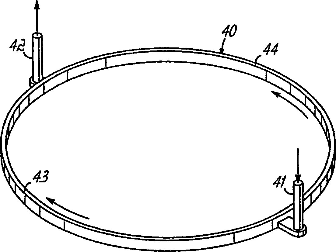
[0029] As shown in FIG. 1, an iPVD device 10 of the type described in the present invention is disclosed in US Patent No. 6,287,435. Apparatus 10 includes a vacuum chamber 11 bounded by chamber walls 14 and having, for processing therein, a semiconductor wafer 12 supported on an upwardly facing substrate support 13 . A source 15 of ionized sputtering material is located at the top of the vacuum chamber 11 and includes a frusto-conical magnetron sputtering target 16 with an RF energy source 20 located within an opening 17 of the target 16 . The RF energy source 20 includes an RF coil or antenna 21 connected to the output of the RF energy source and cooperating with a network 22 . The coil 21 is located in the atmosphere 18 outside the vacuum chamber 11, behind the dielectric window 23 forming a part of the chamber wall 14 of the vacuum chamber 11, which keeps the processing gas on the vacuum side in the vacuum chamber 11 with the atmosphere of the vacuum chamber 11. Isolated o...


PUM


Abstract

An improved deposition baffle, that is provided to protect a dielectric window from conductive deposits, is provided in high-density-plasma apparatus. The baffle has a central circular part having slots cut therein that are interrupted by electrically conductive bridges. Ribs in the body between the slots have cooling fluid channel sections bored therein, which are joined in series by interconnecting channel portions in a peripheral annular part of the baffle to form a continuous serpentine cooling fluid flow path from an inlet to an outlet in the annular peripheral part of the baffle.

Description

[0001] This invention is related to U.S. Patent Nos. 6,080,287, 6,197,165, and 6,287,435, and to pending U.S. patent applications Nos. 09 / 629,515 (filed August 1, 2000), ), and No. 10 / 080,496 (filed February 22, 2002), the entire contents of which are hereby incorporated by reference. technical field [0002] The present invention relates to the use of deposition baffles in plasma processors, and in particular, the present invention relates to the application of high-density plasmas, such as inductively coupled plasma (ICP), in the production of semiconductor devices and integrated circuits to Machines for processing and preparing coatings, especially conductive coatings. The deposition baffle protects dielectric walls and windows of the vacuum processing chamber through which RF energy is coupled into the high density plasma from being coated with deposition material. Background technique [0003] Inductively coupled plasma (ICP) sources are widely used in the semiconducto...

Claims


Application Information

Patent Timeline
Patent Type & Authority Applications(China)
IPC IPC(8): H01J37/32C23C16/507
CPCH01J37/32633C23C16/507H01J37/321C23C14/358
Inventor 约瑟夫·布罗卡马克·凯肖克蒂姆·普罗文彻
Owner TOKYO ELECTRON LTD
Why Eureka
Try Eureka