Method for preparing microlite silicon

A technology of microcrystalline silicon and amorphous silicon thin film, which is applied in the field of silicon materials to convert amorphous silicon into microcrystalline silicon, can solve the problems of low mobility, low photoelectric conversion efficiency, and low growth rate.

Inactive Publication Date: 2006-02-01
CHANGCHUN INST OF OPTICS FINE MECHANICS & PHYSICS CHINESE ACAD OF SCI
View PDF0 Cites 17 Cited by
  • Summary
  • Abstract
  • Description
  • Claims
  • Application Information

AI Technical Summary

Problems solved by technology

The problem in the preparation of microcrystalline silicon μc-Si material by this method is that its growth rate is low (<1A) which is not conducive to reducing manufacturing costs
[0007] The above-mentioned preparation of microcrystalline silicon thin films by direct deposition method has the following problems to varying degrees: the growth rate is low, which is not conducive to reducing the manufacturing cost; the crystallinity is low, about 50%; the mobility is low, and the photoelectric conversion efficiency is low

Method used


Image

  • Method for preparing microlite silicon
  • Method for preparing microlite silicon
  • Method for preparing microlite silicon

Examples


Embodiment Construction

[0019] The present invention will be further described below in combination with specific embodiments.

[0020] A 50nm-thick hydrogenated amorphous silicon film (a-Si:H) was deposited on glass by plasma-enhanced chemical vapor deposition (PECVD), the substrate temperature was 220°C, and the RF power density was 0.03W / cm 2 , the gas flow rate is 15 sccm, and the reaction chamber pressure is 80Pa.

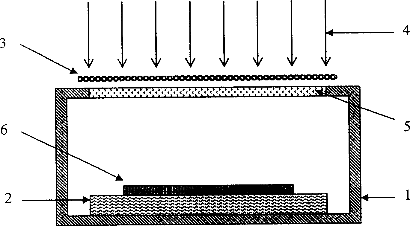
[0021] The above-mentioned hydrogenated amorphous silicon thin film sample 6 is placed on the figure 1 On the heating plate 2 at the bottom of the vacuum annealing furnace 1 shown, after the window 5 is covered, the annealing furnace is evacuated; when the vacuum degree reaches 2Pa, the power supply of the heating plate 2 is turned on for heating, and the ultraviolet light source 4 is turned on at the same time; the sample 6 When the set temperature reaches 400°C, the UV illuminance of the UV light source 4 is stable at 1mW / cm 2 , remove the cover on the window 5, let the ultraviol...


PUM


Abstract

A process for preparing microcrystal silicon includes preparing non-crystal silicon film on glass substrate, putting it in vacuum annealing furnace, and vacuum annealing while radiating it by ultraviolet ray for phase change to obtain microcrystal silicon film. Its advantages are high speed and high crystallinity.

Description

technical field [0001] The invention belongs to the technical field of semiconductor materials and relates to a silicon material, in particular to a method for converting amorphous silicon into microcrystalline silicon. Background technique [0002] The mobility and photoelectric conversion efficiency of microcrystalline silicon are higher than those of amorphous silicon, and compared with polycrystalline silicon, the preparation process is simple and the cost is low, so it is widely used in the preparation of thin film transistors and solar cells. [0003] At present, the method of preparing microcrystalline silicon is mainly direct deposition method, including ultra-high frequency plasma enhanced chemical vapor deposition (VHF PECVD), hot wire chemical vapor deposition (HW CVD) and electron cyclotron resonance chemical vapor deposition (ECR CVD). . [0004] The very high frequency plasma chemical vapor deposition (VHF PECVD) method is based on H 2 Diluted SiH 4 The gas ...

Claims


Application Information

Patent Timeline
Patent Type & Authority Applications(China)
IPC IPC(8): C30B29/06C30B28/02H01L21/34
Inventor 黄金英付国柱荆海凌志华
Owner CHANGCHUN INST OF OPTICS FINE MECHANICS & PHYSICS CHINESE ACAD OF SCI
Why Eureka
Try Eureka