Ultra-thin body super-steep retrograde well (ssrw) fet devices

一种场效应晶体管、超陡后退阱的技术,应用在超薄型本体FET器件领域,能够解决不能实现严格的掺杂分布等问题,达到减小结电容和、减小结泄漏的效果

Active Publication Date: 2006-02-01
GLOBALFOUNDRIES INC
View PDF7 Cites 19 Cited by
  • Summary
  • Abstract
  • Description
  • Claims
  • Application Information

AI Technical Summary

Problems solved by technology

In fact, it has been shown that current silicon processing technologies cannot achieve the tight doping profile that is the goal of changing as far as three orders of magnitude less than 4nm by 2008

Method used


Image

  • Ultra-thin body super-steep retrograde well (ssrw) fet devices
  • Ultra-thin body super-steep retrograde well (ssrw) fet devices
  • Ultra-thin body super-steep retrograde well (ssrw) fet devices

Examples


no. 1 example

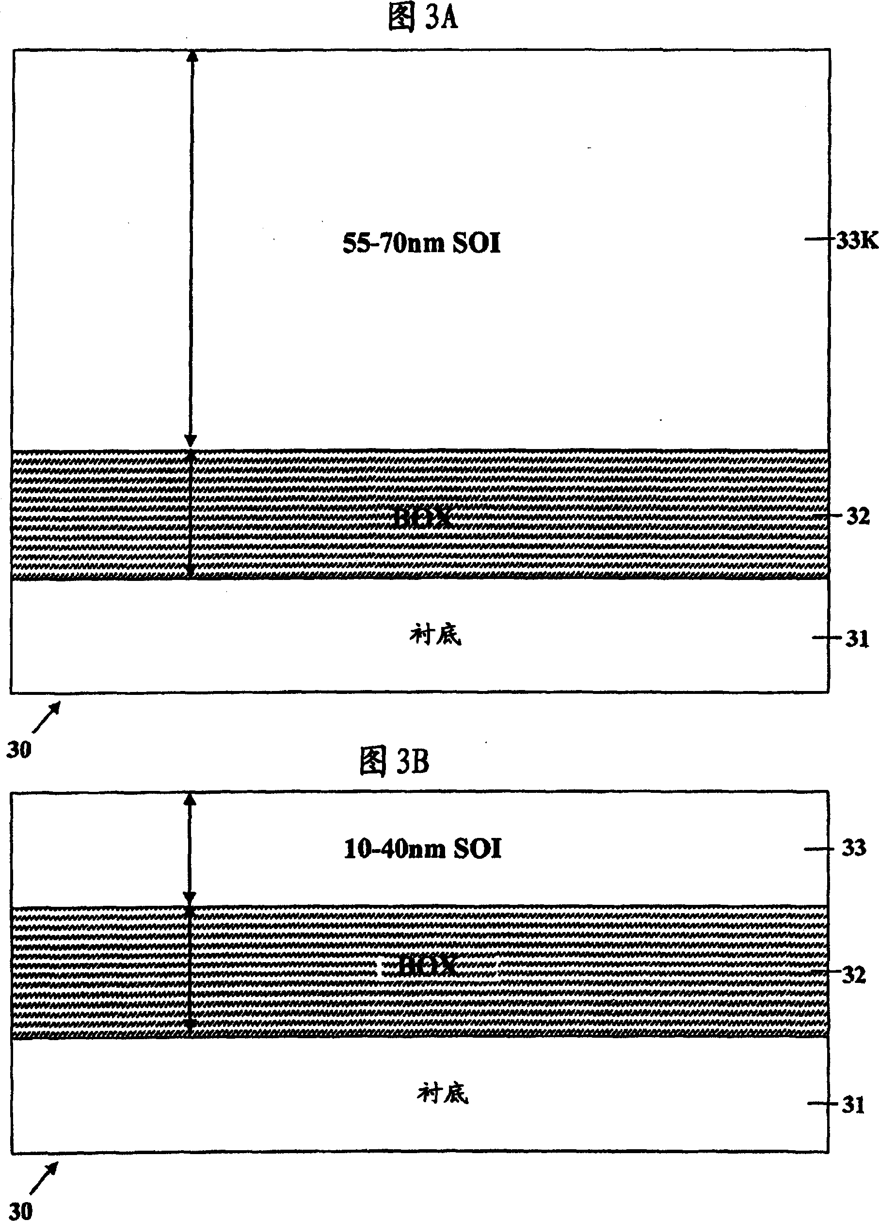
[0065] Figure 4 A flow chart of a first embodiment of the method of the invention is shown. Figure 4 The illustrated process begins (Start) 70 and proceeds to step 71 in which device 30 is processed. The SOI layer 33K initially having a thickness of 55 nm or more on the BOX substrate 31 in FIG. 3A is thinned to an ultra-thin thickness of about 10 nm to 40 nm by the oxidation and lift-off process described above with reference to FIG. 3B.

[0066] At the end of step 71, the desired thickness of the SOI layer 33 has been obtained.

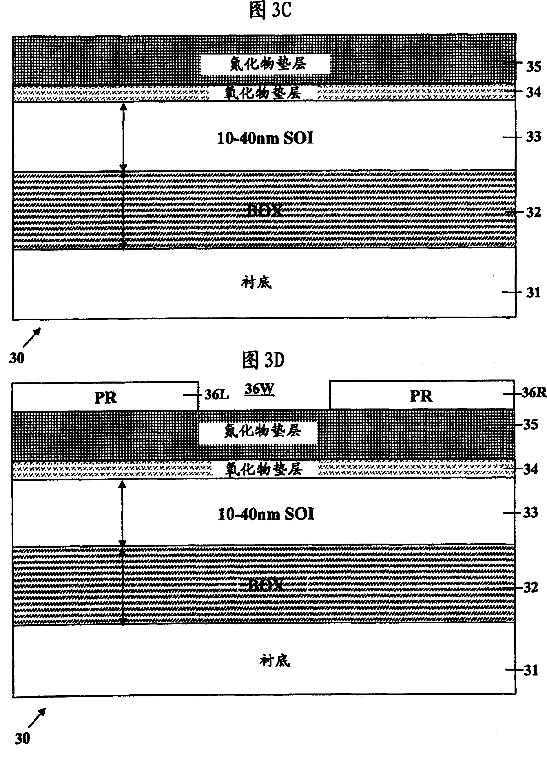
[0067] In step 72 , an oxide pad layer 34 and a nitride pad layer 35 are formed on the thinned SOI layer 33 as shown in FIG. 3C . Next, as shown in FIG. 3D , an isolation image mask 36L / 36R having a central isolation window 36W therein is formed on the nitride pad layer 35 (over the SOI layer 33 ).

[0068]In step 73, isolation trench 37 is formed by etching from the top of device 30 down through isolation window 36W, wherein trench 37 goes dow...

no. 2 example

[0080] Figure 5 A flow chart of a second embodiment of the method of the invention is shown. Figure 5 The illustrated process starts at 90 and proceeds to step 91 in which device 30 is processed. The SOI layer 33K initially having a thickness of 55 nm or more on the BOX substrate 31 in FIG. 3A is thinned to an ultra-thin thickness of about 10 nm to 40 nm by the oxidation and lift-off process described above with reference to FIG. 3B.

[0081] At the end of step 91, the desired thickness of the SOI layer 33 has been obtained.

[0082] In step 92 , an oxide pad layer 34 and a nitride pad layer 35 are formed on the thinned SOI layer 33 as shown in FIG. 3C . Next, as shown in FIG. 3D , an isolation image mask 36L / 36R having a central isolation window 36W therein is formed on the nitride pad layer 35 (over the SOI layer 33 ).

[0083] In step 93, an isolation trench 37 is formed by etching from the top of the device 30 down through the isolation window 36W, wherein the trench...


PUM


Abstract

The present invention provides a method of manufacture of a Super Steep Retrograde Well Field Effect Transistor device starts with an SOI layer formed on a substrate, e.g. a buried oxide layer. Thin the SOI layer to form an ultra-thin SOI layer. Form an isolation trench separating the SOI layer into N and P ground plane regions. Dope the N and P ground plane regions formed from the SOI layer with high levels of N-type and P-type dopant. Form semiconductor channel regions above the N and P ground plane regions. Form FET source and drain regions and gate electrode stacks above the channel regions. Optionally form a diffusion retarding layer between the SOI ground plane regions and the channel regions.

Description

technical field [0001] The present invention relates to a method of manufacturing an ultra-thin body field effect transistor (FET) device and an ultra-thin body FET device manufactured by the method. Background technique [0002] In semiconductor devices such as field effect transistors (FETs) such as complementary metal oxide semiconductor (MOS) FETs or metal-insulator-semiconductor (MIS) FETs, there is a continuing trend towards a steady reduction in the minimum feature size of the devices. Reliable minimum transistor gate circuit lengths on a chip help the microelectronics industry to manufacture products with significant increases in calculable capacity and integration density. [0003] FIG. 1 shows a conventional prior art MOSFET device 10 formed on a P-type doped silicon substrate 11 . A gate dielectric layer 12 (eg, gate oxide) and a gate electrode 14 (eg, polysilicon doped with impurities) are formed as a gate electrode stacked on a top surface of a substrate having...

Claims


Application Information

Patent Timeline
Patent Type & Authority Applications(China)
IPC IPC(8): H01L29/786H01L27/092H01L27/12H01L21/336H01L21/8234H01L21/84
CPCH01L21/76283H01L29/78618H01L29/78696H01L29/66772H01L21/84H01L27/1203H01L21/823892H01L29/78609
Inventor 迪亚尼·C·伯伊德贾德森·R·霍尔特杨美基毛玉莲任志斌哈万·G·沙西迪
Owner GLOBALFOUNDRIES INC
Why Eureka
Try Eureka