Method for preparing high quality GaInAlN material on silicon substrate

A technology of indium gallium aluminum nitrogen and silicon substrates, which is applied in semiconductor/solid-state device manufacturing, electrical components, circuits, etc., can solve problems such as unfavorable indium gallium aluminum nitrogen materials and unstable aluminum transition layers

Inactive Publication Date: 2006-02-15
LATTICE POWER (JIANGXI) CORP
View PDF0 Cites 6 Cited by
  • Summary
  • Abstract
  • Description
  • Claims
  • Application Information

AI Technical Summary

Problems solved by technology

However, due to the low melting point of aluminum (660°C) and the high growth temperature of InGaAlN materials (>1000°C), this aluminum transition layer is unstable during the growth of InGaAlN materials, so it will not Conducive to obtaining high-quality InGaAlN materials

Method used


Image

  • Method for preparing high quality GaInAlN material on silicon substrate

Examples


Embodiment 1

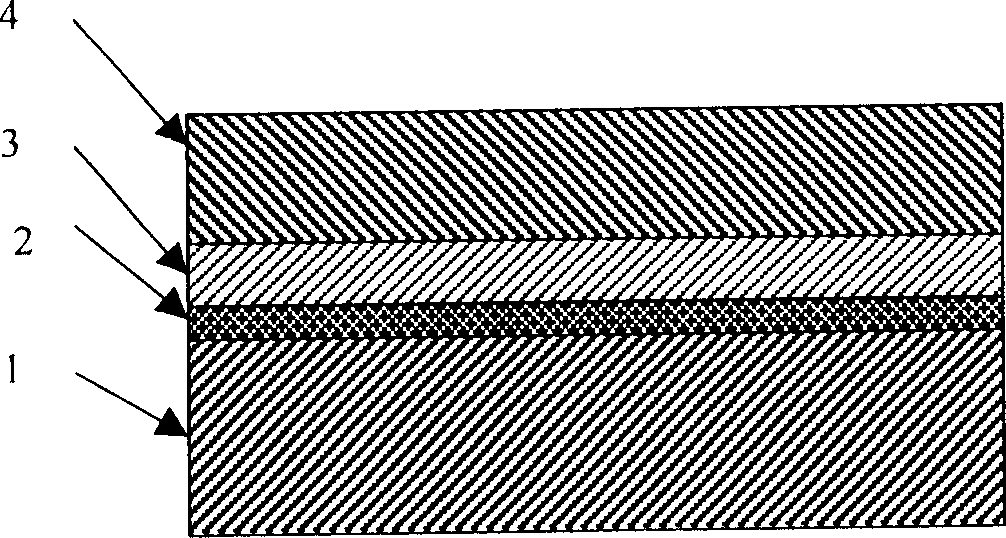
[0012] Clean a silicon (111) substrate 1, put it into the reaction chamber of a metal-organic chemical vapor deposition equipment, firstly treat the surface of the substrate 1 with hydrogen at 1100°C for 5 minutes, and then deposit 30 Å at 800°C Metal titanium transition layer and aluminum nitride low-temperature buffer layer 3 of 200 Å, and then raise the temperature to 1050° C. to grow gallium nitride-doped silicon layer and gallium nitride-doped magnesium layer 4, aluminum nitride low-temperature buffer layer 3 and nitrogen The gallium nitride-doped silicon layer and the gallium nitride-doped magnesium layer 4 constitute an indium gallium aluminum nitride stack.

Embodiment 2

[0014] Clean a silicon (111) substrate 1 and put it into an electron beam evaporation station to deposit a 10 Å titanium metal film, i.e., a titanium transition layer 2, and then put the substrate 1 evaporated with a titanium transition layer 2 into a metal-organic In the reaction chamber of the chemical vapor deposition equipment, the surface of the substrate 1 is first treated with hydrogen gas at 1100°C for 5 minutes, then a 200 Å aluminum nitride low-temperature buffer layer 3 is grown at 800°C, and then the temperature is raised to 1030°C in sequence Growth of undoped gallium nitride layer, silicon-doped gallium nitride layer, indium gallium nitride / gallium nitride multiple quantum well layer, gallium nitride doped magnesium layer 4, aluminum nitride low temperature buffer layer 3 and undoped gallium nitride layer, silicon-doped gallium nitride layer, indium gallium nitride / gallium nitride multiple quantum well layer, and gallium nitride doped magnesium layer 4 constitute ...


PUM


Abstract

This invention discloses a preparation method for high quality material of indium gallium aluminum nitrogen on silicon substrate. For the method, first, forming a titan transition layer on silicon substrate surface, then forming indium gallium aluminum nitrogen stack with at least one low-temperature buffer layer of aluminum nitride that grows directly on titan transition layer. This invention can prevent the harm to metal back of silicon nitride and gallium metal and grow material of high quality.

Description

technical field [0001] The invention relates to semiconductor materials, in particular to a method for preparing high-quality InGaAlN material on a silicon substrate. Background technique: [0002] InGaAlN (In x Ga y Al 1-x-y N, 0<=x<=1, 0<=y<=1) is a preferred material system for preparing short-wavelength light-emitting devices. In recent years, many novel light-emitting devices have been manufactured with InGaAlN materials, such as blue, green, and white light-emitting diodes, purple semiconductor lasers, and so on. At the same time, InGaAlN material is also a good material for preparing many high-performance electronic devices. In the prior art, methods for preparing InGaAlN materials on sapphire substrates and silicon carbide substrates have been relatively mature. According to these disclosed technologies, high-quality InGaAlN materials can already be prepared. However, silicon carbide substrates are very expensive, and the growth of InGaAlN materials...

Claims


Application Information

Patent Timeline
Patent Type & Authority Applications(China)
IPC IPC(8): H01L33/00H01L21/20H01L33/12
Inventor 王立方文卿江风益
Owner LATTICE POWER (JIANGXI) CORP
Why Eureka
Try Eureka