Optical interconnection coupling structure based on soft photoetching

A coupling structure and soft lithography technology, which is applied in the coupling of optical waveguides and other directions, can solve the problems of the alignment tolerance accuracy falling to 0.1-0.3mm, the manufacturing process is complicated, and the mass production is difficult, so as to achieve flexible design and high coupling efficiency. , The effect of easy mass production

Inactive Publication Date: 2006-03-01
ZHEJIANG UNIV
View PDF0 Cites 7 Cited by
  • Summary
  • Abstract
  • Description
  • Claims
  • Application Information

AI Technical Summary

Problems solved by technology

In order for the polymer optical interconnection to be applied to the interconnection between chips (such as printed circuit boards), two key problems need to be solved at the same time: one is how to couple the light beam emitted by the light source to the optical waveguide placed perpendicular to it, and make the light beam Alignment tolerance accuracy drops to 0.1-0.3mm, making practical possible
The main problem that still exists is how to deflect the signal optical path between the optical transmitter module and the optical detector by 90 degrees to more effectively couple with the optical waveguide; the other is how to reduce the reduction in optical signal coupling efficiency due to installation errors
In addition, the complex cost of the manufacturing process of the proposed several methods is too high, and it is difficult to produce in batches.

Method used


Image

  • Optical interconnection coupling structure based on soft photoetching
  • Optical interconnection coupling structure based on soft photoetching
  • Optical interconnection coupling structure based on soft photoetching

Examples


Embodiment Construction

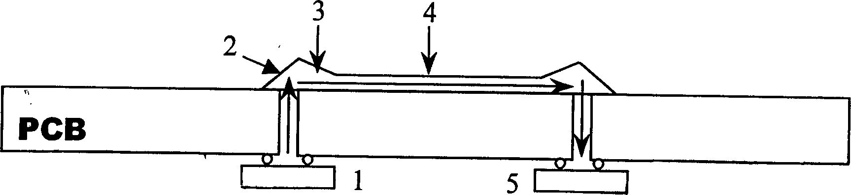
[0018] Such as figure 1 As shown, it includes a light source 1, two reflective surfaces 2, two intermediate coupling sections 3, a square wave guide 4, and an optical receiver 5. A reflecting surface 2 and an intermediate coupling section 3 are connected to one side of the square wave guide 4 in sequence, and the other intermediate coupling setting section 3 and the other reflecting surface 2 are connected to the other side of the square wave guide 4 in sequence , A symmetrically connected connector is installed on the printed circuit board. The printed circuit board has two through holes. The light source 1 and the light receiver 5 are placed on the other side of the printed circuit board. The light source 1 passes through the first through hole. Aligned to one reflective surface 2, the light receiver 5 is aligned to the other reflective surface 2 through the second through hole.

[0019] The light source 1 is a vertical cavity surface emitting laser with an operating wavelength...


PUM


Abstract

The optical interconnection coupled structure based on soft photoetch includes two reflecting surfaces and two intermediate coupled matching sections, they are successively connected on two sides of square waveguide tube, and formed into a symmetrically-connected connection body and mounted on the printed circuit board, on the printed circuit board the through holes are opened, its light source and light receiver are placed on another side of printed circuit board, the light source is aligned with one reflecting surface by means of first through hole, and the light receiver is aligned with another reflecting surface by means of second through hole. The square waveguide tube can be one-step formed by utilizing soft photoetching process. Said structure is applicable to internal short-distance high-speed data transmission in the computer.

Description

Technical field [0001] The invention relates to an optical interconnection coupling structure based on soft lithography. Background technique [0002] With the rapid growth of global communication traffic, business forms are becoming increasingly diversified, image transmission and processing technology is developing day by day, and bandwidth requirements are exploding, requiring each node on the network to provide a higher transmission rate. In the past two decades, optical signals have been widely used as information transmission media for long-distance network transmission. Long-distance communication network systems use parallel optical fibers to connect optical switches, routers, and WDM terminal systems for long-distance network interconnection. On the other hand, the microelectronics industry has greatly improved the performance of electronic circuits to alleviate this problem, but with the high integration of large-scale integrated circuits (LSI) and the increase in data ...

Claims


Application Information

Patent Timeline
IPC IPC(8): G02B6/26G02B6/42
Inventor 吴君豪鲍俊峰吴兴坤
Owner ZHEJIANG UNIV
Why Eureka
Try Eureka