

Bond pad structure
一种接合垫、合金的技术,应用在半导体/固态器件零部件、半导体器件、电气元件等方向,能够解决降低接合可靠性、接合垫间距与尺寸无法进一步缩小、失去与金层线连结等问题,达到增加可靠度、避免失效与接垫剥离的效果
- Summary
- Abstract
- Description
- Claims
- Application Information
AI Technical Summary
Problems solved by technology
Method used
Image

Examples
Embodiment Construction
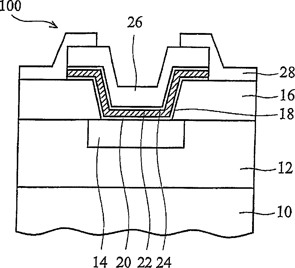
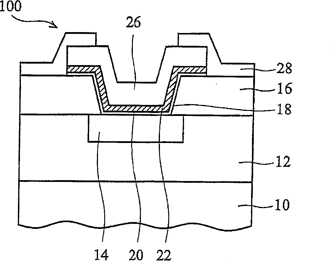
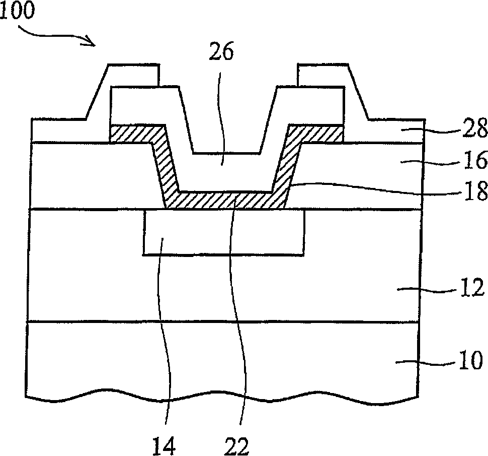
[0032]The present invention provides an improved bond pad structure for integrated circuits. One embodiment of the present invention provides a bonding pad structure, which has a stress buffer layer disposed between an uppermost interconnection metal layer and a bonding pad layer, so as to avoid damage caused by wafer electrical testing (such as wafer The probe test) and the damage caused by the stress of package impact (such as wire bonding, flip-chip packaging or other external forces in the packaging process). The stress buffer layer can be a conductive material, and compared with the material properties of one of the first metal layer and the bonding pad layer, Young's modulus, hardness, strength or toughness of the stress buffer layer (toughness) is larger. In one embodiment of the present invention, a bonding pad structure is provided on an integrated circuit chip having at least one low-k multilayer (dielectric constant substantially less than 3.9), which has a stress ...
PUM
 Abstract
Description
Claims
Application Information