Thin film patterning apparatus and method of fabricating color filter array substrate using the same

A technology of a color filter array and a manufacturing method, which is applied in the directions of optical filters, photolithographic process exposure devices, optics, etc., can solve the problems of a long time, waste of photoresist, increase of manufacturing process time and cost, etc.

Inactive Publication Date: 2006-05-17
LG DISPLAY CO LTD
View PDF0 Cites 27 Cited by
  • Summary
  • Abstract
  • Description
  • Claims
  • Application Information

AI Technical Summary

Problems solved by technology

The photolithography process has problems that it takes a long time, a developing solution for developing the photoresist, wastes too much photoresist, and requires expensive exposure equipment
In addition, the process of forming the ribs 34 and the process of forming the coating layer 22 are separately performed, and thus, there is a problem that the time and cost of the manufacturing process increase.

Method used


Image

  • Thin film patterning apparatus and method of fabricating color filter array substrate using the same
  • Thin film patterning apparatus and method of fabricating color filter array substrate using the same
  • Thin film patterning apparatus and method of fabricating color filter array substrate using the same

Examples


Embodiment Construction

[0051] Preferred embodiments of the present invention will be described in detail with reference to Examples illustrated in the accompanying drawings. Below, will refer to Figures 6 to 17E Preferred embodiments of the present invention are described in detail.

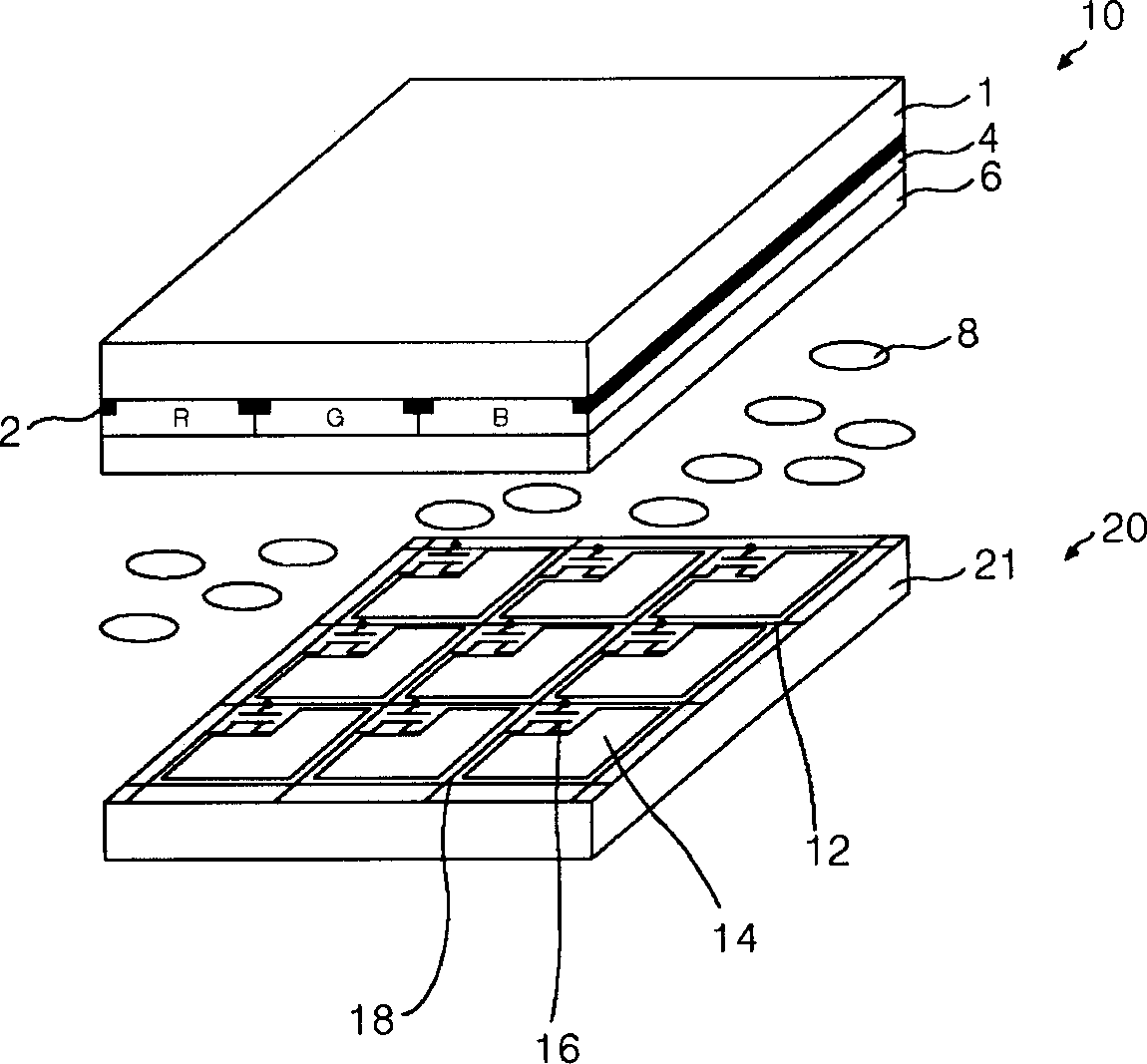
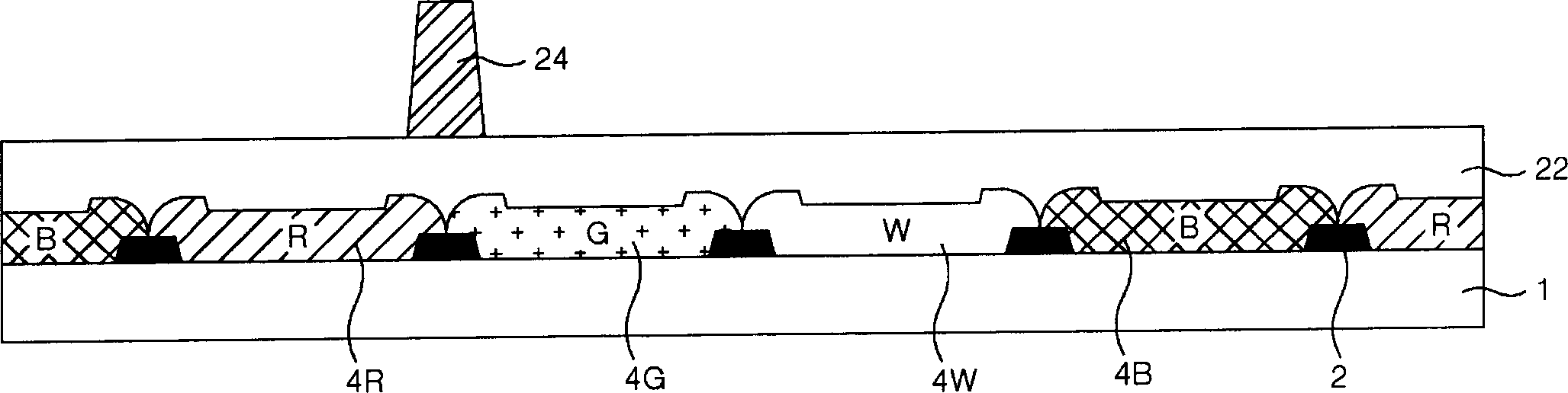
[0052] Figure 6 and 7 are respectively a plan view and a cross-sectional view showing the color filter array substrate according to the first embodiment of the present invention. refer to Figure 6 and 7 , the color filter array substrate according to the first embodiment of the present invention includes a black matrix 102 formed on an upper substrate 101; red, green and blue color filters 104R, 104G and 104B; a coating with a white color filter 104W layer 122; and liner 124 formed on coating layer 122.

[0053] The black matrix 102 is formed on the upper substrate 101 in a matrix form to define a plurality of unit regions forming the color filters 104 and to prevent light interference between adjacent units. ...


PUM


Abstract

The manufacturing method of the color filter array substrate includes the following steps: forming a black matrix on the substrate, forming red, green and blue color filters on the substrate with the black matrix formed thereon, forming red, green and blue color filters on it forming a coating layer containing a white color filter on the substrate of the color filter, aligning the flat soft mold with the coating layer, and using the flat soft mold to planarize the coating layer.

Description

[0001] This application claims the benefit of Korean Patent Application Nos. P2004-92132 and P2004-92133, both filed on November 11, 2004, which are hereby incorporated by reference in their entirety. technical field [0002] The present invention relates to a liquid crystal display device, more particularly to a thin film patterning device and a method for manufacturing a color filter substrate using the device. Although the present invention is applicable to a wide range of applications, it is particularly suitable for a thin film patterning device capable of performing a patterning process without using a photolithography process. Background technique [0003] Generally, a liquid crystal display (LCD) controls light transmittance of liquid crystals by using an electric field, thereby displaying images. A liquid crystal display device includes a liquid crystal display panel in which liquid crystal cells are arranged in a matrix, and a driving circuit for driving the liquid...

Claims


Application Information

Patent Timeline
IPC IPC(8): G02B5/20G02F1/1335G03F7/20
CPCG02F1/1303G02F1/133345G02F1/133514G02F1/133519
Inventor 蔡基成曺奎哲黄龙燮金珍郁李昌熙
Owner LG DISPLAY CO LTD
Why Eureka
Try Eureka