Method for bonding chip with different materials by sealed quartz tube

A quartz glass tube and wafer bonding technology, used in electrical components, semiconductor/solid-state device manufacturing, circuits, etc., can solve the problems of expensive wafer bonding systems and high system maintenance requirements

Inactive Publication Date: 2006-05-31
INST OF SEMICONDUCTORS - CHINESE ACAD OF SCI
View PDF0 Cites 1 Cited by
  • Summary
  • Abstract
  • Description
  • Claims
  • Application Information

AI Technical Summary

Problems solved by technology

[0003] KaulSuss in Germany and EVG in Austria both grow wafer bonding machines, but the co...

Method used


Image

  • Method for bonding chip with different materials by sealed quartz tube
  • Method for bonding chip with different materials by sealed quartz tube
  • Method for bonding chip with different materials by sealed quartz tube

Examples


Embodiment Construction

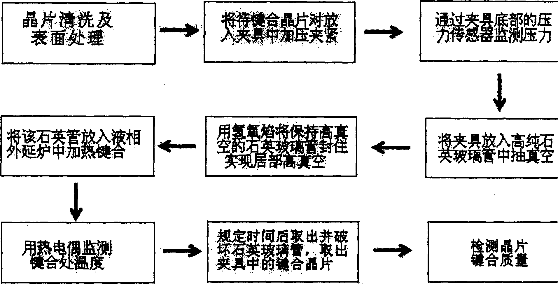
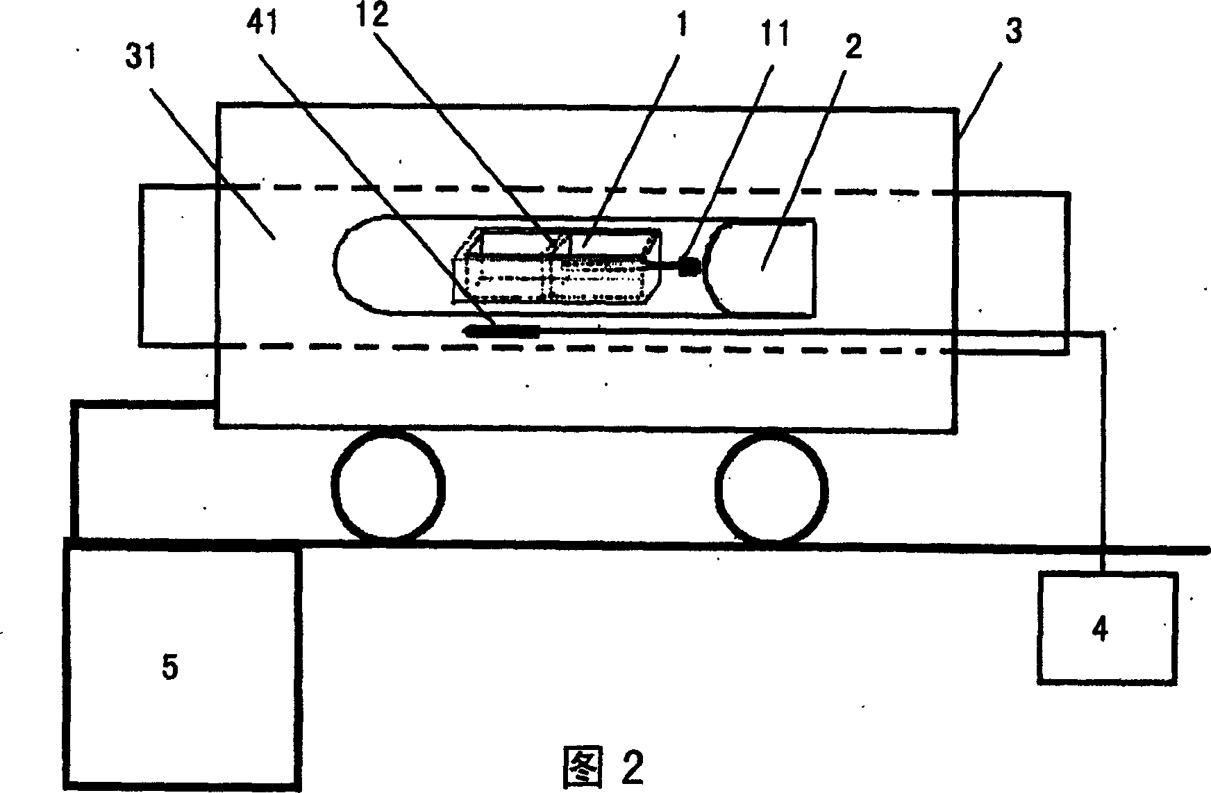
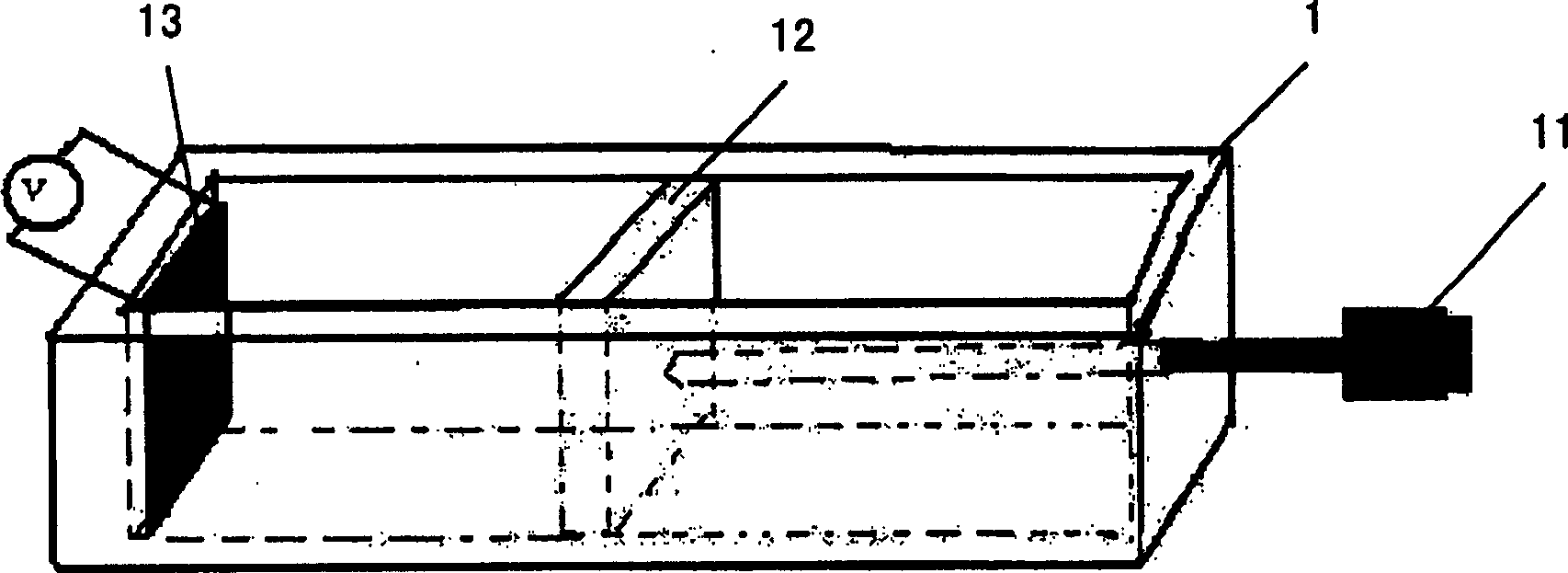
[0020] The present invention utilizes the sealed quartz glass tube to provide local high vacuum to realize the equipment connection mode of wafer bonding such as figure 1 Shown: the sealed quartz glass tube 2 is put into the inner cavity 31 of the liquid phase epitaxy furnace 3, the sealed quartz glass tube 2 is a high vacuum, and the bonding fixture 1 and the wafer (not shown in the figure) are packaged; A nickel-chromium-nickel-silicon thermocouple probe 41 is arranged below the glass tube 2, and the probe 41 is connected to the thermocouple temperature monitor 4; chamber heating temperature.

[0021] The preparatory work for sample processing of wafer bonding includes: cleaning - removing organic contamination; dissolving oxide layer; removing particulate metal contamination while passivating the surface of the wafer. The formulations of the standard wet chemical treatments used are as follows:

[0022] Sulphate H 2 SO 4 :H 2 o 2 (2:1 to 4:1) T=120-140°C, t=10min, use...


PUM


Abstract

A method for bonding the chips made of different materials by use of sealed quartz glass tube includes such steps as cleaning said chips, treating their surfaces, providing fixture used for binding, arranging piezoelectric ceramic at the bottom of fixture for measuring the binding pressure, fixing the chips in the fixture, putting them in high-purity quartz glass tube, vacuumizing it, sealing it by oxyhydrogen flame, arranging the NiCr-NiSi thermoelectric couple at the fixture position in liquid-phase epitaxial furnace for monitoring the binding temp, loading the fixture and chips in the liquid-phase epitaxial furnace, and heating at 300-800 deg.C for 10 min-24 hr.

Description

technical field [0001] The invention relates to the technical field of wafer bonding, and is a method for realizing wafer bonding of different materials by using a sealed quartz glass tube to provide local high vacuum, and is suitable for realizing III-V materials and Si-Si, Si-III-V groups Bonding of materials. Background technique [0002] Two wafers with flat and clean surfaces can be bonded to each other through chemical bonds on the surface under certain conditions, without being limited by the crystal lattice and crystal orientation of the two wafer materials. This is the wafer bonding technology. Using bonding technology to combine new structural materials has a great degree of freedom, so it is widely used in microelectronic circuits, sensors, power devices, micromachining, optoelectronic devices, silicon-on-insulator wafers (SOI) and other fields. Wafer bonding technology has become a technology that can be used to fabricate many important optoelectronic devices. ...

Claims


Application Information

Patent Timeline
IPC IPC(8): H01L21/00H01L21/02
Inventor 杨国华孙永伟何国荣肖雪芳
Owner INST OF SEMICONDUCTORS - CHINESE ACAD OF SCI
Why Eureka
Try Eureka