Method for mfg. large power MOS tube with small wire wide slot type structure

A MOS tube and trench type technology, which is applied in the field of manufacturing high-power MOS tubes with a small line width trench structure, can solve problems affecting devices, device threshold voltage drift, etc., to reduce thermal processes and improve landfill performance Effect

Active Publication Date: 2006-06-14
SHANGHAI HUAHONG GRACE SEMICON MFG CORP
View PDF0 Cites 6 Cited by
  • Summary
  • Abstract
  • Description
  • Claims
  • Application Information

AI Technical Summary

Problems solved by technology

When the MOS tube is shrunk, the distance from the contact hole to the channel becomes shorter, and the lateral diffusion of the contact hole injection during borophosphorus glass reflow will affect the channel region, thereby affecting the threshold voltage of the device, resulting in a shift in the threshold voltage of the device

Method used


Image

  • Method for mfg. large power MOS tube with small wire wide slot type structure
  • Method for mfg. large power MOS tube with small wire wide slot type structure

Examples


Embodiment Construction

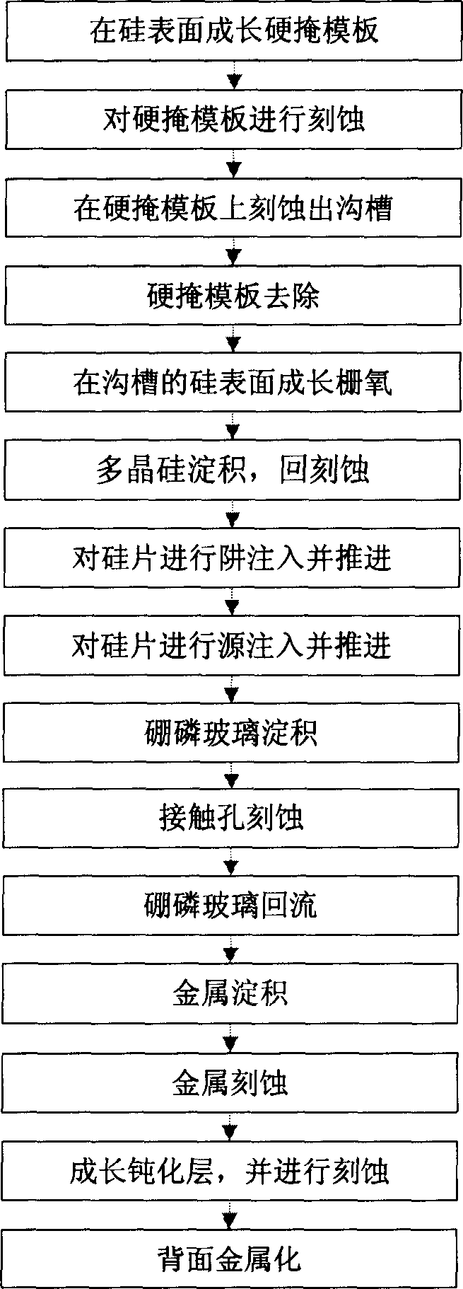
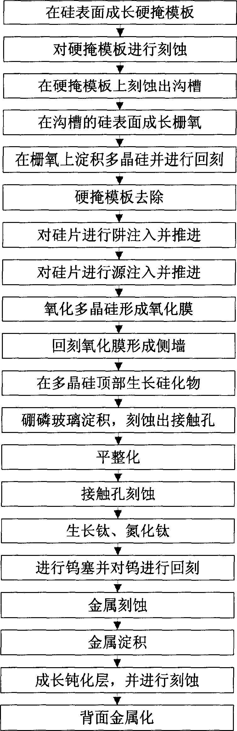
[0012] Such as figure 2 As shown, a hard mask is grown on the silicon surface, and a trench with an aperture of 0.4um-0.6um and a depth of 1um-2um is formed on the silicon surface by plasma etching. The hard mask used in etching is WJ-SIO with a thickness of 2000nm-3000nm 2 . After the trench is formed, the hard mask is not removed temporarily. A gate oxide film with a thickness of 10nm-50nm is formed by thermal oxidation. Then, 800nm-1200nm polysilicon is deposited by low pressure chemical vapor deposition and etched back to the surface of the hard mask. By means of ion implantation, the well area of ​​the silicon wafer is implanted and advanced, and the source area of ​​the silicon wafer is implanted and advanced; an oxide film with a thickness of 100nm-200nm is formed on the polysilicon by oxidation. Etching back the previously grown oxide film to form sidewall structures on the two sidewalls of the protruding polysilicon. Growth of silicide on top of polysilicon, gro...


PUM

PropertyMeasurementUnit
thicknessaaaaaaaaaa
thicknessaaaaaaaaaa
thicknessaaaaaaaaaa

Abstract

The invention discloses a method for manufacturing small-linewidth grooved high-power MOS tube, adopting titanium alloy process to reduce the effect of contact hole injection on device characteristics and the contact resistance, and adopting chemical-mechanical polishing and leveling process to reduce the thermal process of B-P glass deposition and backflow so as to reduce the effect of the transverse diffusion of the contact hole injection on the device characteristics; and adopting W plug process to improve the burying property of a small-size contact hole. The invention can be used to semiconductor manufacturing.

Description

technical field [0001] The invention relates to a method for manufacturing a MOS tube, in particular to a method for manufacturing a high-power MOS tube with a small line width trench structure. Background technique [0002] Deep trench structure high-power MOS transistors have become the development trend of high-power MOS transistors. Most of the high-performance and high-power MOS tubes now adopt this structure. Most of the current high-power MOS transistors with deep trench structure have a primary cell size of 2.4um to 3.2um. With the continuous reduction of cost requirements and the continuous improvement of current density requirements for power devices, the continuous reduction of the original cell size has become a trend. The original cell size gradually develops to 1.6um or even smaller. [0003] With the continuous shrinking of the size, the existing deep trench MOS manufacturing method can no longer meet the requirements of the reduced device size. [0004] I...

Claims


Application Information

Patent Timeline
Patent Type & Authority Applications(China)
IPC IPC(8): H01L21/336
Inventor 陈志伟居宇涵
Owner SHANGHAI HUAHONG GRACE SEMICON MFG CORP
Why Eureka
Try Eureka