Method for mounting an electronic component on a substrate

A technology of electronic devices and assembly methods, which is applied in the direction of assembling printed circuits with electrical components, electrical solid devices, printed circuits connected with non-printed electrical components, etc., and can solve problems such as fracture, rupture, and strain of connecting parts

Inactive Publication Date: 2006-06-14
NAGRAVISION SA
View PDF3 Cites 0 Cited by
  • Summary
  • Abstract
  • Description
  • Claims
  • Application Information

AI Technical Summary

Problems solved by technology

[0011] Although these devices are protected by coating or laminating insulating films, the connections of these devices are subject to inherent tension and compression when the transponder deforms, causing them to rupture
This phenomenon is further exacerbated during repeated deformations, causing strain in the connection that will eventually break after the transponder is subjected to a small amount of bending or twisting

Method used


Image

  • Method for mounting an electronic component on a substrate
  • Method for mounting an electronic component on a substrate
  • Method for mounting an electronic component on a substrate

Examples


Embodiment Construction

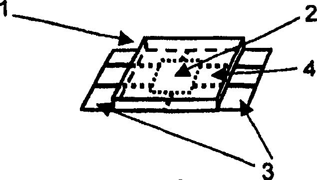
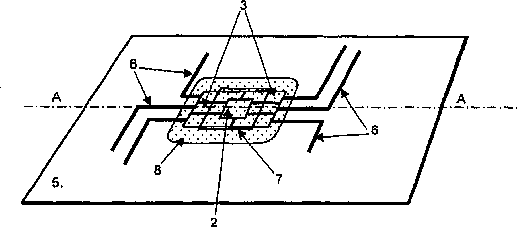
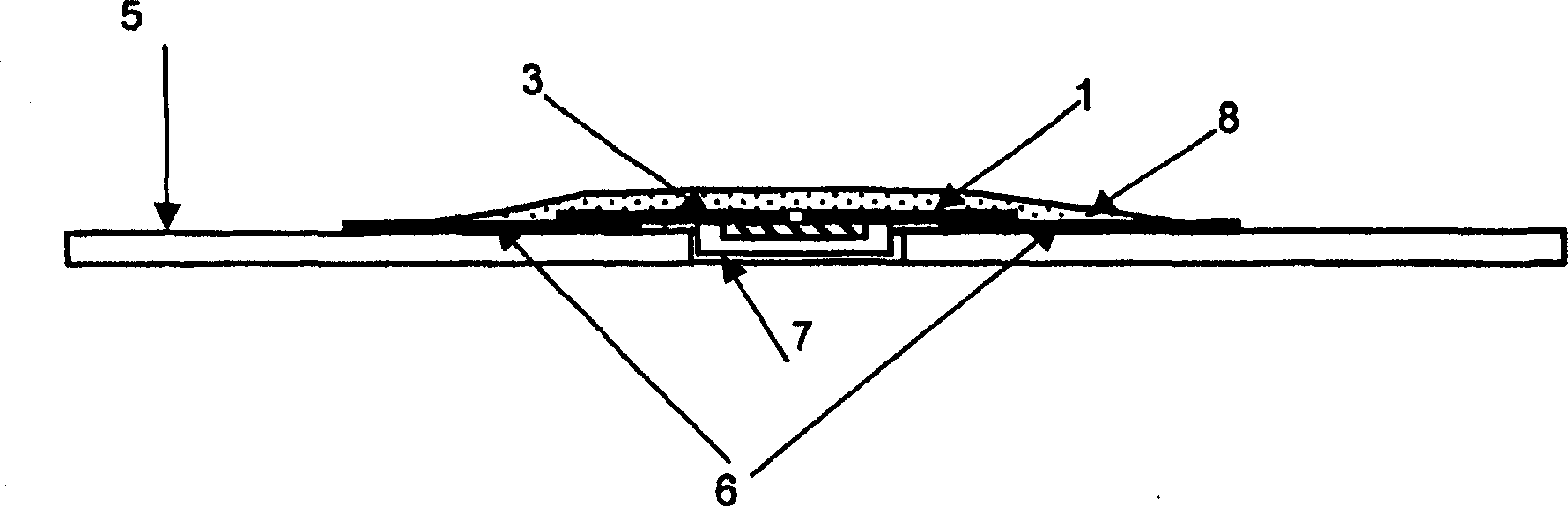
[0029] form a transponder in the figure 1 The device (1) in comprises a chip (2) protected by an insulating material such as an epoxy coating (4). The chip contacts are connected to contact areas (3) formed eg inside a tinned copper conductive plate forming a "lead frame".

[0030] figure 2 and in image 3 The cross-section according to the axis A-A shown shows an embodiment of a transponder comprising the figure 1 Deformable thin substrate (5) of device (1) in . The upper surface of the substrate comprises tracks or conductive areas (6) that are etched, glued or printed, for example by screen printing. The coated part (4) of the device (1) is inserted into a cavity (7) formed by milling or cutting a window out of the substrate in order to reduce the final thickness of the transponder. The conductive traces (6) of the substrate are in contact with the conductive areas (3) of the device only by pressure without soldering or conductive glue. The approximately flat surface...


PUM


Abstract

This invention proposes a manufacturing process for a transponder in the form of a card or a label able to resist to flexions or twisting without interrupting the connections of the electronic components. The process of assembling at least one electronic component including sensibly flat conductive areas that are connected to conductive tracks placed on the surface of a generally flat substrate comprises the steps of placing the substrate on a work surface, the face including conductive tracks being oriented upwards, placing the electronic component into a cavity of the substrate situated in a zone including the conductive tracks, the conductive areas of the component coming into contact with the corresponding tracks of the substrate and applying a layer of insulating material which extends at once on the electronic component and at least on a substrate zone surrounding said component. This process implies that the contact between the conductive areas of the electronic component and the conductive tracks of the substrate realizes an electric connection ensured by the pressure of application of the insulating material layer on the electronic component.

Description

technical field [0001] The present invention relates to an assembly method for mounting electronic components on an insulating support called a substrate comprising a plurality of conductive tracks. The method can be used in the manufacture of transponders in the form of cards or electronic tags, which are generally of low thickness. Background technique [0002] An electronic tag is considered to refer to an assembly comprising at least one insulating support, an antenna and an electronic device, usually a chip. Cards or electronic tags produced using the method according to the invention are found in many applications as means of identification, control or payment. [0003] The subject of the invention is in particular the assembly of at least one electronic device on a thin card or label. An electronic device is a component such as a chip, a capacitor, a resistor, a diode, a fuse, a battery, a display, or also a coated chip comprising contact areas. [0004] Cards or c...

Claims


Application Information

Patent Timeline
Patent Type & Authority Applications(China)
IPC IPC(8): G06K19/077B23K1/00H05K1/18H05K3/28H05K3/32
CPCB23K1/0008G06K19/07728G06K19/07745G06K19/07749H05K1/182H05K3/284H05K3/325H05K2201/10727H05K2203/1311H01L2924/0002B23K2101/40H01L2924/00H05K13/00H05K13/04
Inventor 弗朗西斯·德罗茨
Owner NAGRAVISION SA
Why Eureka
Try Eureka