Light-emitting diode and method of preparing the same

A technology of light-emitting diodes and electrodes, applied in semiconductor devices, electrical components, circuits, etc., can solve the problems of insufficient current expansion, low light-emitting efficiency, uneven light-emitting, etc., to improve external quantum efficiency, increase light-emitting area, and reduce output. corner effect

Active Publication Date: 2006-06-21
EPILIGHT TECH +1
View PDF0 Cites 23 Cited by
  • Summary
  • Abstract
  • Description
  • Claims
  • Application Information

AI Technical Summary

Problems solved by technology

Due to the staggered structure of its electrodes, if there is a slight deviation in the production, the staggered structure is not uniform and symmetrical, which will lead to insufficient current expansion, resulting in uneven light emission, and the light output area is small, and there is a limitation of total reflection angle, and the light output efficiency is low.

Method used


Image

  • Light-emitting diode and method of preparing the same
  • Light-emitting diode and method of preparing the same
  • Light-emitting diode and method of preparing the same

Examples


Embodiment Construction

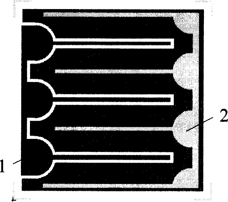
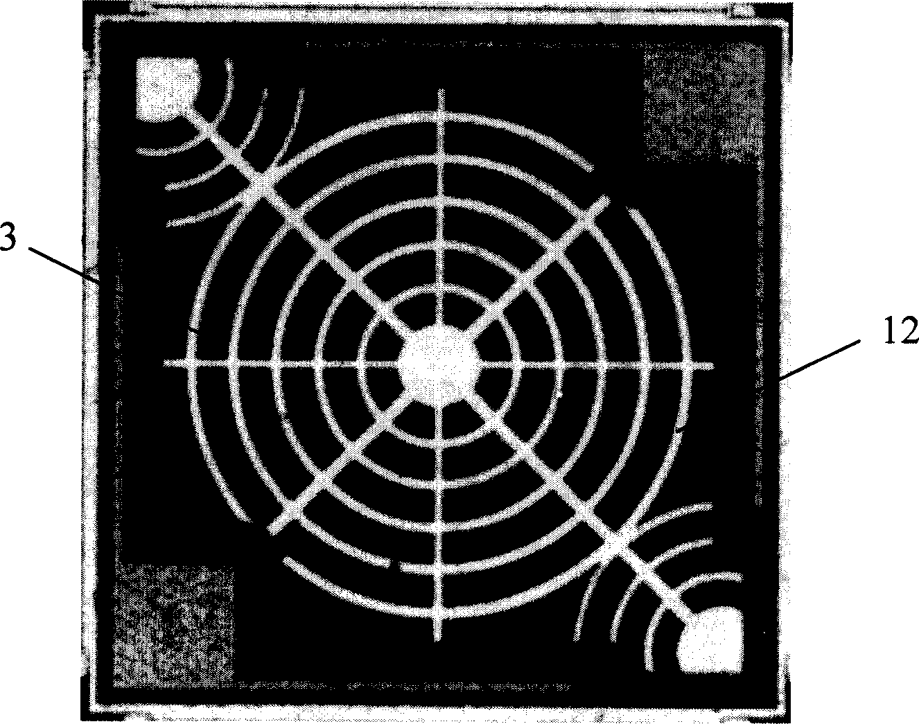
[0025] A light-emitting diode of the present invention, comprising a sapphire substrate 4, a GaN nucleation layer 5, a GaN buffer layer 6, an n-type GaN ohmic contact layer 7, an InGaN / GaN quantum well active layer 8, and a p-type AlGaN carrier blocking layer 9. A p-type GaN ohmic contact layer 10 , a p-type ohmic-contact transparent electrode 11 , an n-type ohmic-contact electrode 13 , and a p-type ohmic-contact electrode 12 . The p-type ohmic contact electrode 12 is a concentric circular structure, such as image 3 , in order to make full use of the light emitting area, a plurality of p-type ohmic contact electrodes 12 with concentric circle structures are integrated on the same chip. There is a groove 3 between the p-type ohmic contact electrodes 12. The groove 3 increases the probability of side light emission and the light emission area, avoiding light being absorbed by the material and electrodes (including the p-type ohmic contact transparent electrode 11), and the ring...


PUM


Abstract

The invention discloses a LED, which comprises: a sapphire substrate, a GaN buffer layer, an N/P-type GaN/ohmic contact layer, an InGaN/GaN quantum trap active layer, and a concentric P-type ohmic contact transparent electrode with grooves between near ring electrodes manufactured by dry etching. This invention makes even current injection, increases probability of side-surface light, reduces reflection angle, and thereby decreases greatly light energy loss.

Description

technical field [0001] The invention relates to a light emitting diode, in particular to a light emitting diode based on gallium nitride semiconductor material. The invention also relates to a preparation method of the light emitting diode. Background technique [0002] Semiconductor light-emitting diodes have a wide range of applications in the fields of full-color large-screen image display, optical storage, sign recognition, underwater and space communications, medical equipment, photoelectric integration, and military reconnaissance. In particular, gallium nitride-based blue, violet, and ultraviolet semiconductor light-emitting diodes can be used as the basic light source of white light tubes, and have the advantages of energy saving, greenness, and environmental protection. It has broad application prospects and huge market demand. [0003] Semiconductor light-emitting diodes inject current into the active layer located at the P-N junction, and emit light through the ...

Claims


Application Information

Patent Timeline
Patent Type & Authority Applications(China)
IPC IPC(8): H01L33/00H01L33/38
Inventor 张国义陈志忠丁晓民秦志新胡晓东童玉珍董志江靳彩霞李树明
Owner EPILIGHT TECH
Why Eureka
Try Eureka