Panel display having adulterated polycrystal silicon field emission cathode array structure and its manufacturing technology

A flat-panel display and array structure technology, applied in cold cathode manufacturing, electrode system manufacturing, discharge tube/lamp manufacturing, etc., can solve the problems of increasing the overall cost of the device, improve the success rate of manufacturing, simplify the manufacturing process, and improve integration degree of effect

Inactive Publication Date: 2006-06-28
ZHONGYUAN ENGINEERING COLLEGE
View PDF0 Cites 30 Cited by
  • Summary
  • Abstract
  • Description
  • Claims
  • Application Information

AI Technical Summary

Problems solved by technology

This puts higher requirements on the insulating layer in terms of technology and

Method used


Image

  • Panel display having adulterated polycrystal silicon field emission cathode array structure and its manufacturing technology
  • Panel display having adulterated polycrystal silicon field emission cathode array structure and its manufacturing technology
  • Panel display having adulterated polycrystal silicon field emission cathode array structure and its manufacturing technology

Examples


Embodiment Construction

[0047] The present invention will be further described below in conjunction with the accompanying drawings and embodiments, but the present invention is not limited to these embodiments.

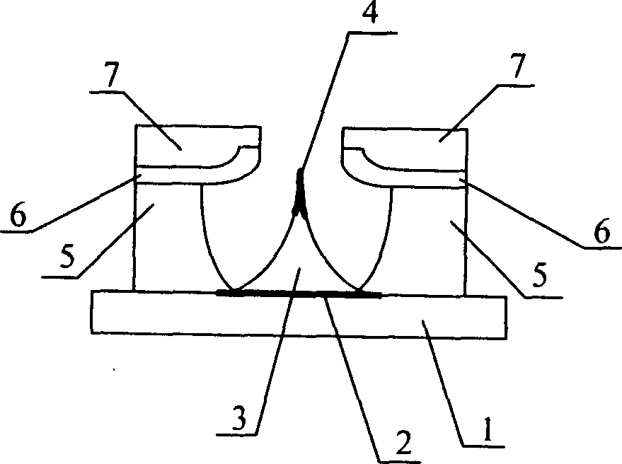
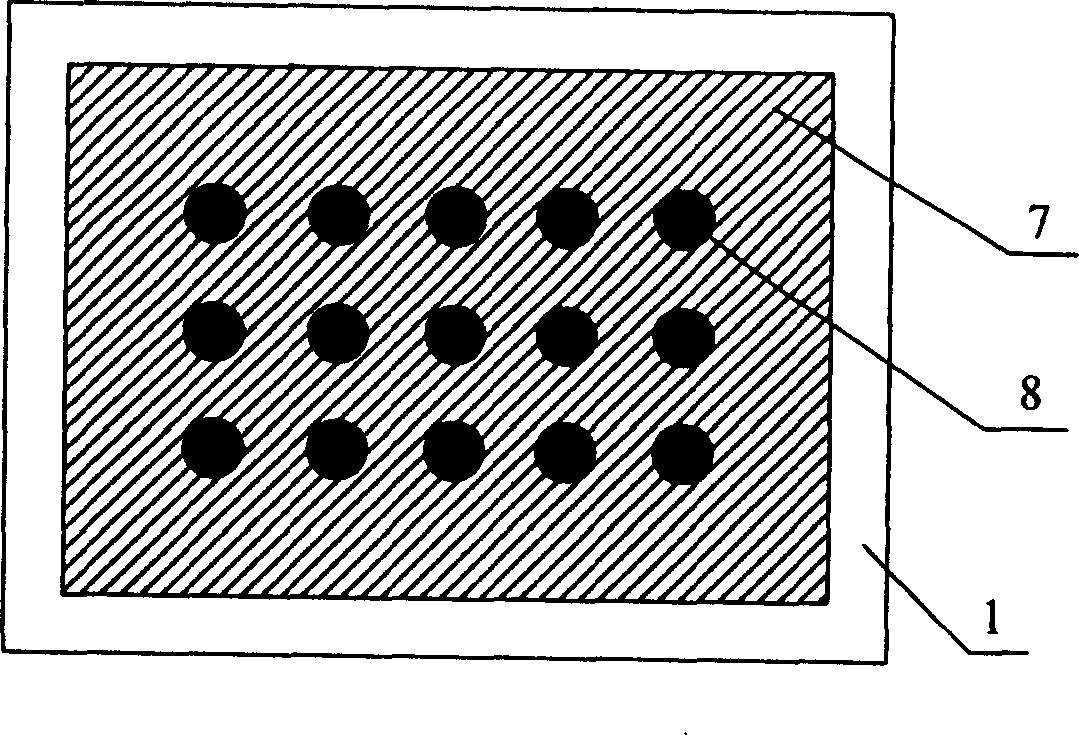
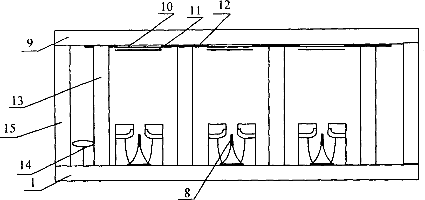
[0048] Such as image 3 Shown, the present invention comprises the sealed vacuum chamber that is made of cathode panel 1 (i.e. substrate material glass 1), anode panel 9 and surrounding glass enclosing frame 15; On anode panel 9, the anode conductive strip 10 of photoetching out and making Phosphor powder layer 11 on the anode conductive strip 10; insulating paste layer 12 printed on the non-display area of ​​the anode conductive strip 10; supporting wall 13 and getter accessory element 14 arranged between the cathode panel 1 and the anode panel 9 , a doped polysilicon field emission cathode array structure is fabricated on the cathode panel 1 . On the cathode panel, there are doped polysilicon field emission cathode array structure and carbon nanotube cathode; the control gate used to cont...


PUM


Abstract

This invention relates to a panel display with doped-polysilicon field emission cathode array structure and its process technology, in which, the display includes a sealed vacuum cavity composed of a cathode panel, an anode panel and surrounding glasses, anode conduction strips etched on the anode panel and fluorescence powder layer on the conduction strips, a supporting wall and getter attached elements, in which, a doped polysilicon field emission cathode array structure is prepared on the cathode panel to reduce the distance between the cathode and the grating, control the working voltage of the grating and reduce the current of the control grating.

Description

technical field [0001] The invention belongs to the fields of plane display technology, microelectronic science and technology, vacuum science and technology, and nano science and technology, and relates to the manufacture of flat panel field emission displays, in particular to flat panels for carbon nanotube cathodes. The device manufacturing aspect of the field emission display particularly relates to the manufacturing process of a field emission flat display device with a doped polysilicon field emission cathode array structure and a carbon nanotube cathode. Background technique [0002] Carbon nanotubes have a small tip curvature radius, high aspect ratio, good field emission characteristics and excellent physical and chemical stability. Carbon nanotubes themselves are coaxial, tubular substances that emit large amounts of electrons when an applied voltage is applied. The flat panel display using carbon nanotubes as the cathode material is a new type of field emission d...

Claims


Application Information

Patent Timeline
IPC IPC(8): H01J29/04H01J1/304H01J31/12H01J9/02
Inventor 李玉魁
Owner ZHONGYUAN ENGINEERING COLLEGE
Why Eureka
Try Eureka