Stepped and repeated illuminating and nano-imprinting device

A nano-imprint and pressure technology, which is applied in the direction of optics, opto-mechanical equipment, and photoplate-making process on patterned surfaces, can solve the problems of inability to make overprint multi-layer nanostructure graphics, imperfect equipment technology, and poor alignment and overprinting accuracy. High-level problems, to achieve the effect of large imprinting effective area, low price and easy operation

Active Publication Date: 2006-07-12
INST OF OPTICS & ELECTRONICS - CHINESE ACAD OF SCI
View PDF0 Cites 22 Cited by
  • Summary
  • Abstract
  • Description
  • Claims
  • Application Information

AI Technical Summary

Problems solved by technology

The former needs to increase the temperature and pressure, and at the same time lower the temperature below the glass temperature of the polymer. The expansion coefficients of the stamper and the substrate are different, and the deformation during the embossing process makes it difficult to align and overprint the graphics. And it seems insufficient; the latter steps into flash embossing, which avoids the shortcomings of the for

Method used


Image

  • Stepped and repeated illuminating and nano-imprinting device
  • Stepped and repeated illuminating and nano-imprinting device
  • Stepped and repeated illuminating and nano-imprinting device

Examples


Embodiment Construction

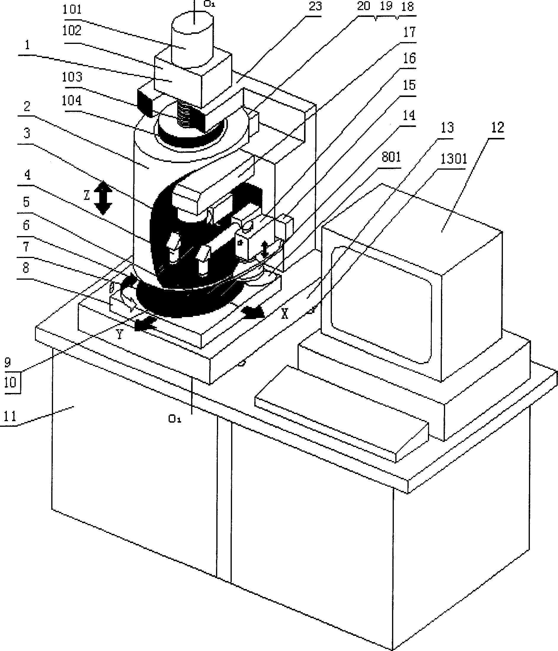
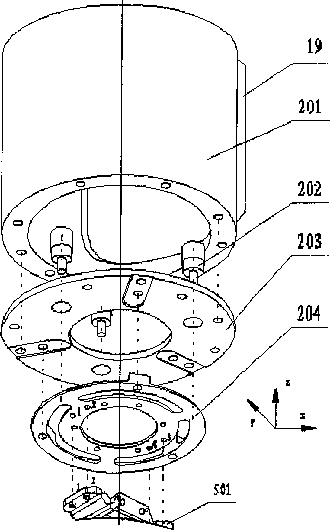
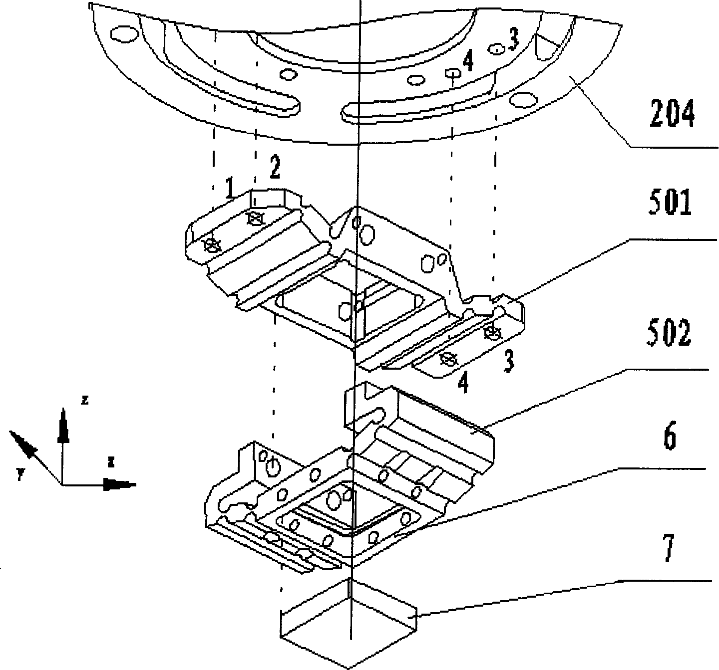
[0036] Such as figure 1 As shown, the present invention consists of a pressure drive system 1 composed of a motor, motor drive and transmission, a Z-direction calibration mechanism 2, a dual-channel CCD alignment system 4, an inclination calibration mechanism 5, a die chuck 6, a die 7, XYθ workpiece table 8, substrate 9, substrate support leveling system 10, large machine cabinet 11, computer system 12, main machine base plate 13, air seal 14, droplet device 15, air seal seat 16, purple light uniform illumination The system 17, the Z-direction measurement sensor 18, the Z-direction linear guide including the inner guide rail 19 and the outer guide rail 20, the Z-direction lifting and lower movement limiters 21 and 22 at both ends, and the frame 23 are composed of parts. The large base plate 13 of the main machine is placed on the large table of the large machine cabinet 11 through the vibration isolation pad 1301, and the large machine cabinet 11 is placed including the consta...


PUM


Abstract

The invention discloses a nanometer stamping device of process repeated illumination, which comprises the following parts: pressure driving system, Z-direction calibration system, two-way CCD aligning system, inclined calibration structure, stamper, substrate, XYª’ working table, substrate bearing piece leveling system, big machine cabinet, control system, big host floor, violet even illuminating system and rack, wherein the bearing piece leveling system is set on the XYª’ working table to load substrate; the pressure driving system, Z-direction calibration system, inclined calibration structure, two-way CCD aligning system and violet even illuminating system are fixed on the rack. The invention adapts common violet illumination without elastic signet or casting mould as well as adding high temperature, pressure and reducing temperature, which applies the high precise alignment of CCD image to make more complex multiple-layer structure, large effective working area and easy extended nanometer image structure through process repeated manufacturing.

Description

technical field [0001] The invention is a step-by-step and repeated illumination nano-imprinting device, which belongs to the field of nano-graphic structure devices produced by micro-processing technology. Background technique [0002] With the rapid development of global communication technology and high-tech information technology, there is an urgent need for microfabrication technology to produce ultra-high-speed, ultra-high-frequency nanoscale IC devices, and the production of nano-pattern structures requires a substantial increase in the resolution of existing lithography technology . Generally, methods of shortening wavelength lithography are used, mainly including deep ultraviolet light, extreme ultraviolet light, X-ray, ion beam projection, and electron beam lithography. These methods all require an extremely short-wavelength light source electromagnetic radiation system and an optical system, which are technically very complicated, and at the same time, the invest...

Claims


Application Information

Patent Timeline
IPC IPC(8): G03F7/00H01L21/027
Inventor 罗先刚陈旭南胡承刚
Owner INST OF OPTICS & ELECTRONICS - CHINESE ACAD OF SCI
Why Eureka
Try Eureka