Solder interconnect structure and method using injection molded solder

一种焊料、电连接的技术,应用在焊接/切割介质/材料、焊接设备、制造工具等方向,能够解决硅器件功率增加、机械应力增加、不允许芯片和衬底充分隔离等问题

Inactive Publication Date: 2006-08-16
INT BUSINESS MASCH CORP
View PDF1 Cites 16 Cited by
  • Summary
  • Abstract
  • Description
  • Claims
  • Application Information

AI Technical Summary

Problems solved by technology

Second, the increase in silicon chip size also limits the ability of underfill to enhance conventional ball solder interconnects
Third, the power required for silicon devices increases, especially for microprocessor chips; and conventional solder interconnects are unlikely to withstand the high currents required to deliver this power
This relieves the stress on the solder bump itself, but adds a processing step, which is time consuming and adds cost
As signal and power demands increase, the smaller spherical size of each bump does not allow adequate isolation between the chip and substrate, which has two detrimental effects
First, capillary underfill processes become slow or infeasible; second, increased mechanical stress due to CTE mismatch
In addition, such underfill layers are generally opaque, thus preventing optical communication between the bottom of chip 20 and substrate 22, as desired in advanced packaging schemes

Method used


Image

  • Solder interconnect structure and method using injection molded solder
  • Solder interconnect structure and method using injection molded solder
  • Solder interconnect structure and method using injection molded solder

Examples


example 1

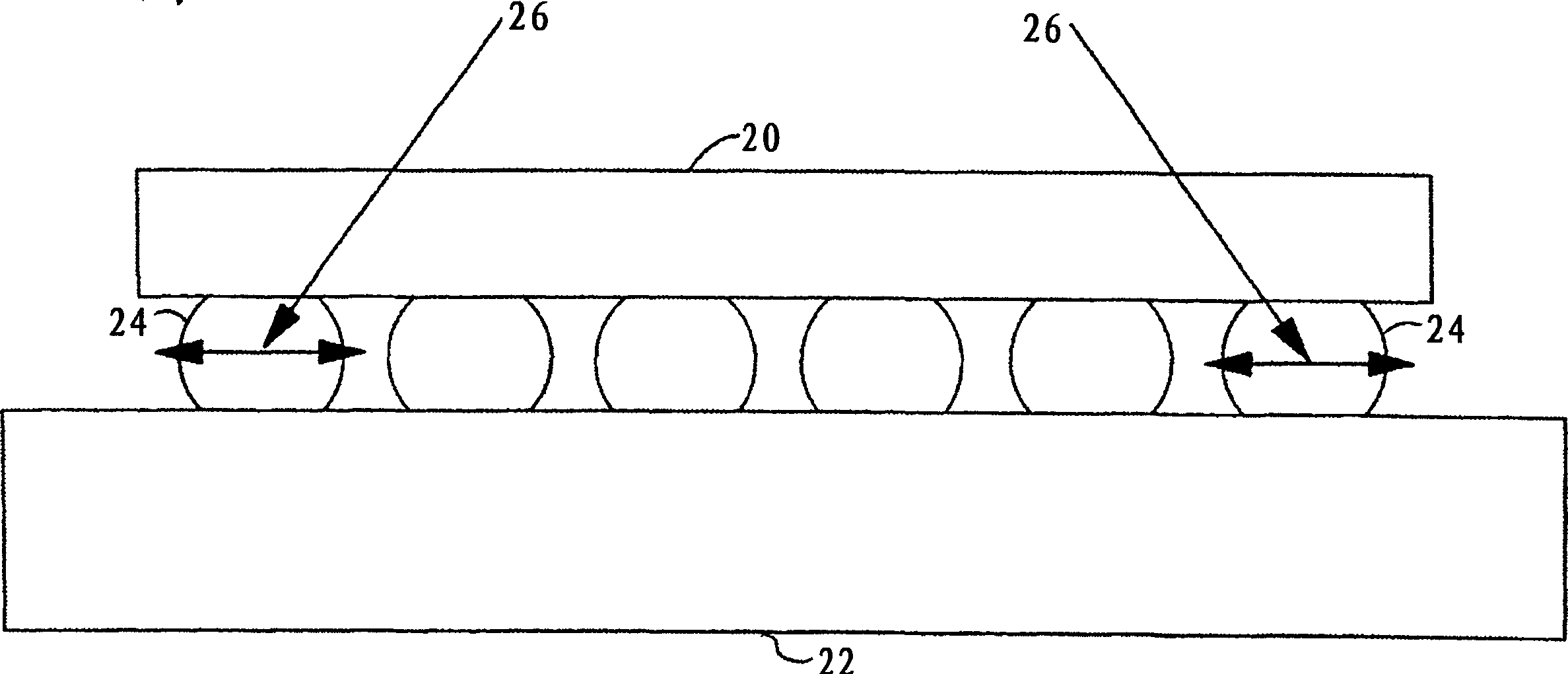
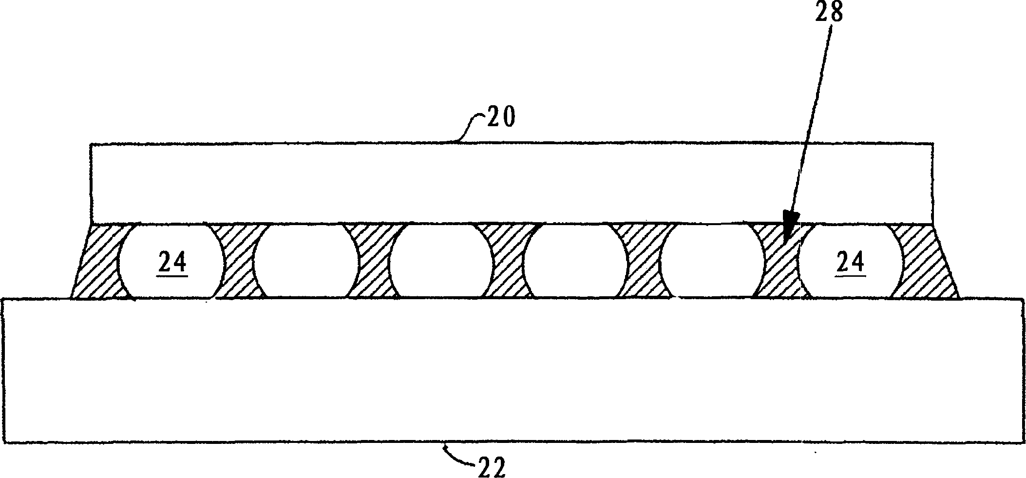
[0058] A preferred structure for improved flip chip interconnection may have cylindrical solder pillars with a diameter of 25-150 microns, preferably 50-100 microns. The interconnection may be 100-600 microns long, with an aspect ratio of length to diameter of 1.5:1-10:1, preferably in the range of 2:1 to 4:1. The manufacturing method of the interconnection will be described below.

[0059] The rectangular or square mold plates are patterned into an array with preferably cylindrical cavities. The mold plate can be a combination of borosilicate glass or a laser-processed polymer layer and glass. For example, in the United States Patent Application Serial No. 10 / XXXXXX, the name is: Combination Solder Transfer Mold Plate Structure and Its Manufacturing Method, Attorney Docket No . YOR920030189 US1, this document is granted the same assignee as the present invention and is incorporated in this application for reference. In addition, the size of the die plate may include 200mm or 300m...

example 2

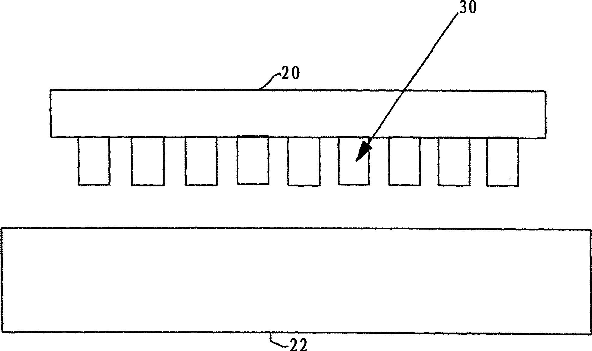
[0063] Another preferred structure for improving flip-chip interconnection is that copper wires with a diameter of 25-100 microns are buried in solder pillars with a diameter of 50-150 microns. The interconnection can be 100-600 microns long with an aspect ratio of length to diameter of 1.5:1-10:1, preferably in the range of 2:1 to 4:1. The manufacturing method of the interconnection will be described below.

[0064] The rectangular or square mold plates are patterned into an array with preferably cylindrical cavities. The mold plate can be a combination of borosilicate glass or a laser-processed polymer layer and glass. For example, in the United States Patent Application Serial No. 10 / XXXXXX, the name is: Combination Solder Transfer Mold Plate Structure and Its Manufacturing Method, Attorney Docket No . YOR920030189 US1, this document is granted the same assignee as the present invention and is incorporated in this application for reference. In addition, the size of the die plat...


PUM

PropertyMeasurementUnit
melting pointaaaaaaaaaa

Abstract

Improved interconnects are produced by injection molded solder which fills mold arrays with molten solder so that columns that have much greater height to width aspect ratios greater than one are formed, rather than conventional flip chip bumps. The columns may have filler particles or reinforcing conductors therein. In the interconnect structures produced, the cost and time of a subsequent underfill step is reduced or avoided. The problem of incompatibility with optical interconnects between chips because underfills require high loading of silica fillers which scatter light, is solved, thus allowing flip chips to incorporate optical interconnects.

Description

Technical field [0001] The present invention relates to the field of solder interconnections formed between a circuit device and a substrate forming the next level of electrical interconnection. In particular, the present invention relates to improvements in the injection molding solder technology used to form solder bump interconnections generally on silicon wafers. Background technique [0002] Semiconductor chips are usually connected to other circuits using solder bumps with a diameter of about 100 microns. These solder joints suffer from thermal fatigue failure because of the difference in coefficient of thermal expansion (CTE) between the silicon and the chip carrier that holds them. Using injection molding solder (IMS) technology, solder interconnections can be fabricated on semiconductor chips or chip carriers with controlled shapes and compositions, thereby extending the fatigue life of the joint. Therefore, the present invention aims to improve the solder interconnectio...

Claims


Application Information

Patent Timeline
Patent Type & Authority Applications(China)
IPC IPC(8): B23K1/00H05K3/34H01L21/60
CPCH01L24/12H01L2224/13082H01L2224/13184H05K2201/10287H05K2201/10992H01L2924/01082H01L2924/01004H05K3/3436H05K3/3426H01L2924/01322H01L2924/01029H01L2924/01044H01L2224/13655H01L2924/00013H01L2224/13147H01L2224/13181H01L2924/01027H01L2224/13639H01L24/11H01L2224/13644H01L2924/014H01L2224/32225H05K2203/128H01L2224/1357H01L2924/01047H01L2924/01079H01L2224/73204H01L2224/1308H01L2224/13155H05K2203/0113H01L2924/14H01L2224/13176H01L2924/01005H01L2924/01033H01L2924/01006H05K2203/0415H05K3/3468B23K35/26H01L2924/01074H01L2924/01078H01L2924/10253H01L2924/01073H01L2224/131H01L2224/16225H01L2224/0554H01L2224/05568H01L2224/05573H01L2924/00014H01L2924/15787Y02P70/50H01L2224/13099H01L2924/00H01L2224/05599H01L2224/0555H01L2224/0556
Inventor 斯蒂芬·L·布奇沃尔特史达原(音译)康圣权皮特·A·格鲁伯克劳蒂奥·菲格尔保罗·A·劳罗
Owner INT BUSINESS MASCH CORP
Why Eureka
Try Eureka