Bonding method and apparatus

A bonding method and bonding device technology, applied in the bonding method of adhesive heating, printed circuit dielectrics, transparent dielectrics, etc., can solve the problems of time-consuming bonding, complicated control, and easy conduction of heat to other components. Achieve high-speed and high-precision mounting, and suppress warping and unevenness

Inactive Publication Date: 2006-08-16
ORMON CORP
View PDF1 Cites 16 Cited by
  • Summary
  • Abstract
  • Description
  • Claims
  • Application Information

AI Technical Summary

Problems solved by technology

[0030] However, since the ACF is basically welded by heat conduction, it is necessary to continue heating the ACF for a predetermined period of time, and there is a problem that joining takes time.
Also, the longer it takes for bonding, the easier it is for heat to be conducted to other constituent elements, which may cause failure
[0031] Furthermore, although the cooling process for suppressing the temperature gradient is disclosed, it is difficult to control the cooling process, requiring complicated control

Method used


Image

  • Bonding method and apparatus
  • Bonding method and apparatus
  • Bonding method and apparatus

Examples


no. 1 approach

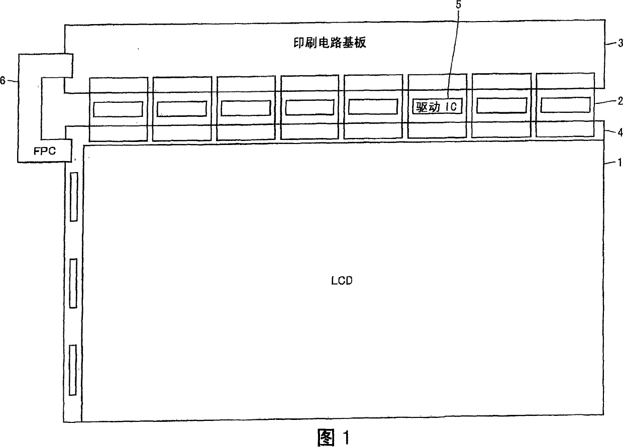
[0061] FIG. 1 is a schematic block diagram illustrating a liquid crystal display device according to a first embodiment of the present invention.

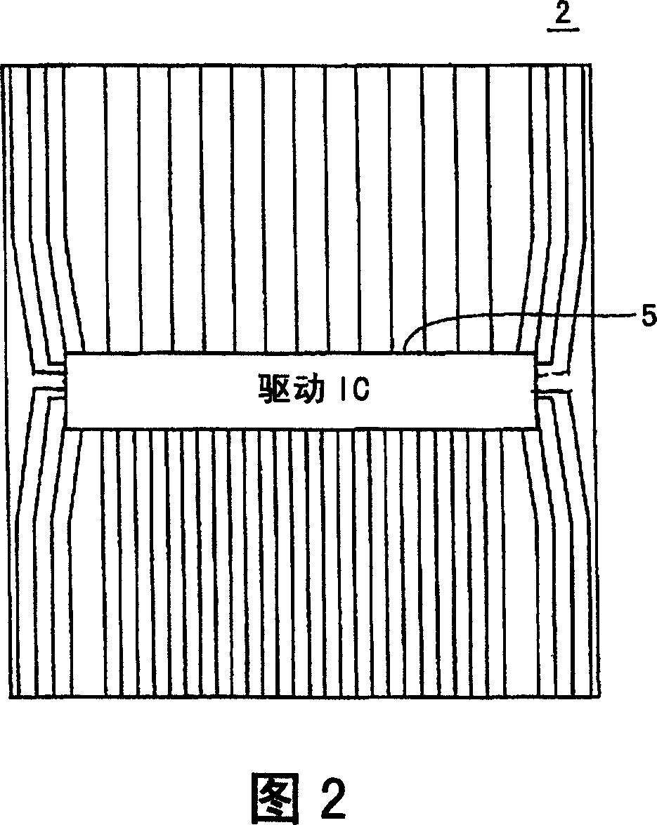
[0062] As shown in FIG. 1 , the liquid crystal display device according to the first embodiment of the present invention includes: a liquid crystal display panel (hereinafter also referred to as LCD) 1; Set on the periphery of LCD1; printed circuit board 3, which is used to drive the liquid crystal material mounted on the LCD; TCP2, which is arranged between the printed circuit board 3 and the liquid crystal display panel LCD1, including the composition for driving the liquid crystal display panel A drive IC 5 for the element; a flexible substrate (hereinafter also referred to as FPC) 6 for electrically connecting the printed circuit board 3 and the interface portion 4 .

[0063] Hereinafter, regarding the bonding apparatus according to the embodiment of the present invention, the bonding method of TCP including the driver IC 5 use...

no. 2 approach

[0113] In recent years, along with the development of microfabrication technology, the wiring pitch has also been significantly narrowed. Along with this, high-precision joining is required. However, a certain degree of variation in the manufacturing stage must also be taken into consideration, and it is generally necessary to design the wiring pitch and the like in consideration of the variation in the manufacturing stage. That is, it is necessary to design the wiring pitch with a certain degree of safety factor.

[0114] In the second embodiment of the present invention, an alignment correction method that enables highly accurate bonding even when the wiring pitch is further reduced will be described.

[0115] FIG. 10 is a diagram illustrating alignment correction according to the second embodiment of the present invention.

[0116] Here, a case where the lower electrode on the TCP side is joined to the upper electrode on the array substrate (glass substrate) side will be ...


PUM

PropertyMeasurementUnit
areaaaaaaaaaaa

Abstract

The invention provides a bonding device capable of shortening a bonding time and performing high speed and accurate mounting by irradiating a laser to an anisotropic conductive film (ACF) which is a mounting adhesive. Laser generated from a laser generator is reflected by a laser mirror, passes through an array substrate (glass substrate) through a backup glass, and then, directly irradiated to an ACF in a pinpoint manner. The laser from the laser generator is set to have a wavelength whose transmittance of transmitting the TCP and the array substrate having the ACF inserted therebetween is higher than that of the other wavelength. The ACF is welded by this laser irradiation, so that the TCP and the array substrate are bonded to each other.

Description

technical field [0001] The invention relates to a bonding device suitable for bonding a liquid crystal display panel and a driving circuit substrate. Background technique [0002] In recent years, liquid crystal display devices have been rapidly popularized as image display devices for personal computers and other various monitors. [0003] Such a liquid crystal display device generally arranges a backlight as a planar light source for illumination on the back of the liquid crystal display panel to irradiate the liquid crystal surface with a predetermined area with uniform brightness as a whole, so as to meet the requirements of the lighting conditions formed on the liquid crystal surface. The visibility of the image. [0004] The liquid crystal display device includes: a liquid crystal display panel, which is formed by sealing a liquid crystal material between two glass substrates; a printed circuit board, which drives the liquid crystal material mounted on the liquid crys...

Claims


Application Information

Patent Timeline
Patent Type & Authority Applications(China)
IPC IPC(8): G02F1/1333G02F1/133G09G3/36
CPCC09J5/06H05K3/361H01L21/67138C09J2400/143C09J11/00H05K2203/107C09J9/00H05K2201/0108C09J2205/31H05K2203/0278H05K3/323C09J2301/416G02F1/1345
Inventor 児岛荣作和田竹彦
Owner ORMON CORP
Why Eureka
Try Eureka